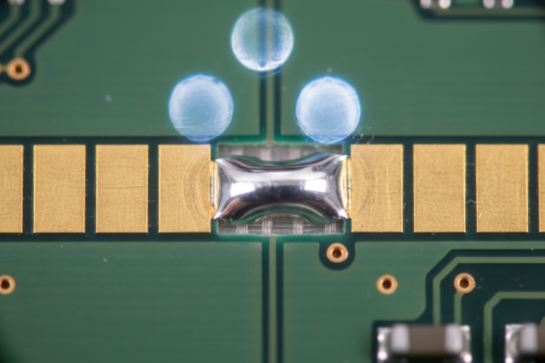
The most expensive sound in electronics manufacturing is the silence of a board that should have booted. When you put that dead board under the microscope, expecting to see a blown capacitor or a backwards diode, you often find something much more insulting: a microscopic bridge of solder connecting two pins on a 0.4mm pitch connector. A $2 manufacturing defect just scrapped a $500 assembly.
Most designers immediately blame the assembly house. They assume the stencil apertures were too wide or the reflow profile too hot. But usually, the failure was baked in months ago during the layout phase, when a decision was made to ignore the physical reality of liquid solder. If there is no physical barrier between two pads, solder will try to merge. That is a law of physics, and strictly enforced.
The Physics of the Bridge
When solder paste melts in the reflow oven, it stops being a gritty paste and becomes a fluid with high surface tension. It wants to minimize its surface area. Ideally, it wets to the pad and the component lead, forming a proper fillet. But on fine-pitch components—anything below 0.5mm pitch—the pads are dangerously close. If the solder mask dam (that thin strip of insulation between pads) is missing, nothing stops that molten fluid from reaching out to its neighbor.
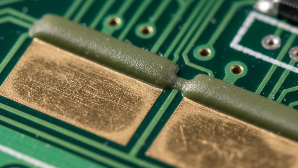
Some engineers try to solve this by “starving” the joint—reducing the stencil aperture to deposit less paste. It’s a common band-aid, often suggested in forums when someone is trying to save a bad layout. While reducing paste volume can lower the probability of a bridge, it doesn’t eliminate the mechanism of failure. If you have a 0.4mm pitch BGA or QFN and rely solely on surface tension to keep the solder in place, you are gambling. A slight misalignment, a vibration in the oven, or a minor variance in flux activity will cause the solder to wick across the gap. The only thing that reliably stops this capillary action is a physical wall: the solder mask dam.
The Geometry of the Sliver
The problem is that you can’t just draw a dam and expect it to exist. Solder mask is a physical material—usually a Liquid Photoimageable (LPI) epoxy—that has to be printed, cured, and developed. Like any material, it has a breaking point. If you design a sliver of mask that is too thin, it won’t adhere to the FR4 substrate. It will peel off during manufacturing, floating away in the developer tank or, worse, flaking off later to contaminate the assembly.
This is where the “Pink Ring” or “Purple Ring” errors in your CAD tool come from. When your DRC (Design Rule Check) flags a “Mask Sliver” violation, it isn’t trying to annoy you. It is telling you that the geometry you requested is physically impossible for the standard chemical process to create.
Standard fabrication processes typically require a minimum mask dam of 4 mils (approx. 0.1mm) to guarantee adhesion. Advanced “HDI” shops might push this down to 3 mils. But look at the math for a 0.4mm pitch component. If the pads are 0.25mm wide, the gap between them is only 0.15mm (approx. 6 mils). If you need a 4 mil dam, and you need to account for mask expansion (registration tolerance) so the mask doesn’t climb onto the pad, you are out of room. You have simply run out of physical space for the insulation.
This geometry trap gets significantly worse if you prioritize aesthetics. We see designs where the enclosure is open, so the industrial designer demands “Matte Black” solder mask to look “premium.” Matte black masks are often softer and require different chemical processing than standard green. They hold heat differently and often have worse adhesion for fine features. A dam that holds perfectly in standard green gloss might flake off in matte black. We have seen entire production runs of 5,000 units hit a 35% failure rate simply because the cool-looking black mask couldn’t hold the 3-mil web between the connector pins. Physics does not care if your board looks cool.
The Gang Relief Trap
When the geometry gets too tight—say, on a 0.35mm pitch BGA or a poorly designed QFN footprint—the fabrication house will send you an “EQ” (Engineering Question). They will point out that they cannot print the dam between the pads. Their proposed solution is almost always “Gang Relief” (or “Gang Masking”).
Gang relief means they simply remove the mask between the pads entirely, creating one large window opening around a row of pins. This satisfies the manufacturing constraint: there is no thin sliver of mask to peel off. But it introduces a catastrophic assembly risk.
Without the dam, you have created a highway for solder. On a QFN (Quad Flat No-lead) package, the solder can wick along the bottom of the package between pins. This type of bridge is insidious because it often hides underneath the component body, invisible to standard AOI (Automated Optical Inspection). You might only find it when the board fails functional test, or worse, when X-ray inspection reveals the short.
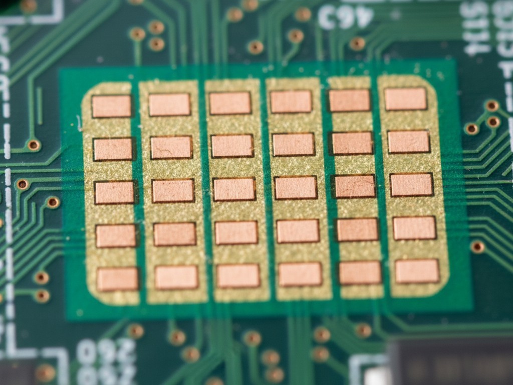
There is a long-term reliability cost here, too. The solder mask doesn’t just stop bridges; it insulates the copper. If you gang relieve a fine-pitch connector, you leave bare FR4 exposed between energized pins. In high-humidity environments, or if the device is not perfectly cleaned of flux residues, that gap becomes a breeding ground for dendritic growth. We have seen medical recalls triggered not by immediate failure, but by dendrites growing across the gang-relieved gap after six months in the field. The dam is an insulator; removing it is a concession to failure.
The “Standard Capability” Fiction
So why do fab houses push for gang relief? Because it protects their yield, not yours. If they try to print a 2.5 mil dam and it peels, they have to scrap the bare board. If they gang relieve it, the bare board passes their electrical test perfectly (because the pads aren’t bridged yet). The bridge happens at your assembly house, which is no longer the bare board fab’s problem.
You have to understand that fab datasheets are often marketing fiction. When a budget offshore fab lists “3 mil mask dam” as a capability, that is their “golden sample” number—what they can achieve on a perfectly calibrated machine with fresh chemistry on a good day. It is not their Cpk > 1.33 process capability. If you send a design with 3 mil dams to a “Standard” pool service, they will often silently remove the dams via a CAM script if they feel they can’t hold them. You won’t know until the boards arrive and the dams are missing.
The solution often involves money. Standard LPI processes use film artwork and UV light, which has alignment and diffraction limits. To reliably hold a sliver on a 0.4mm pitch part, you often need LDI (Laser Direct Imaging). LDI skips the film and uses a laser to cure the mask directly on the board. It is far more precise and can hold tighter dams. It also costs more. When you are arguing with a procurement manager who wants to move the board to a cheaper vendor to save $0.40 per unit, you need to calculate the cost of the scrap. Saving $200 on PCB fabrication is a hollow victory if you lose $4,000 in silicon and technician time reworking bridges on the first 100 boards.
Defensive Design Strategy
The most dangerous setting in your CAD tool is the global “Mask Expansion” rule. Junior engineers often set this to a “safe” 4 mils globally. On a large 0805 resistor, that’s fine. On a 0.4mm pitch component, that global rule will overlap the mask openings and delete your dams without you even realizing it.
You must use local rules. Fine-pitch components require their own specific mask expansion settings, often tightened down to 2 mils or even 1:1 (zero expansion) if the fab capability allows it. You have to force the geometry to permit a 3 or 4 mil dam.
But the ultimate defense happens after the design is done. When you generate your Gerbers, do not trust the 3D viewer. Open the raw GTS (Top Solder Mask) file. Zoom in on your tightest component. Measure the physical gap between the mask openings. If that number is less than 3 mils (approx 0.075mm), you are in the danger zone.
If you see that danger zone, you have two choices: switch to a fab with verified LDI capabilities that can hold that sliver, or change the component footprint. Do not let the fab delete the dam. Do not let them talk you into gang relief on a connector unless you are willing to accept the yield loss. If the fab says “we can’t print this,” believe them. But don’t let them fix it by removing the protection. Move the design, or move the fab. No dam, no build.
