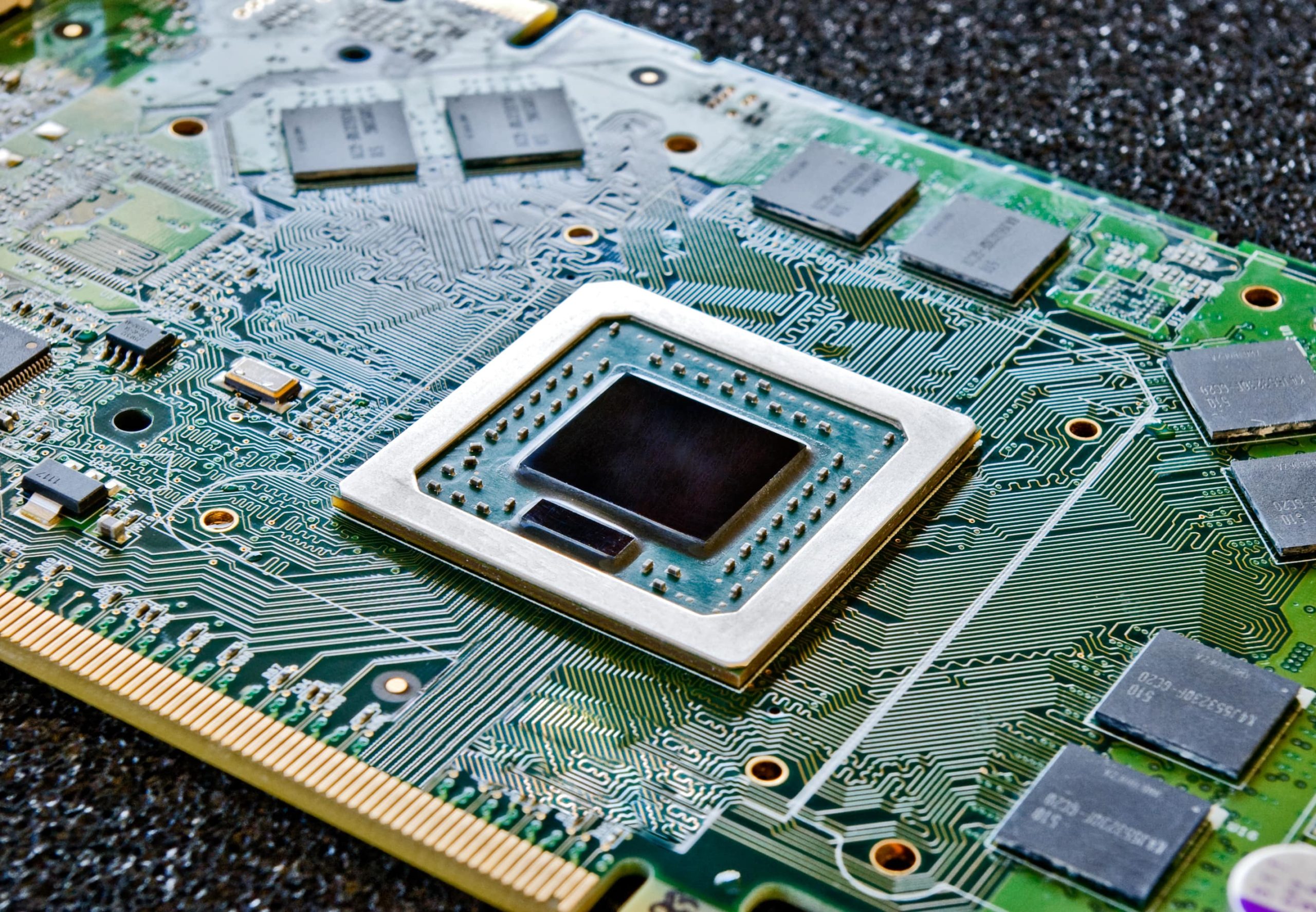
HDI PCB
Experience the Cutting-Edge Technology of HDI PCBs for Unparalleled Precision and Performance
HDI PCB
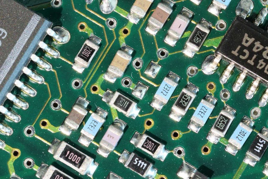
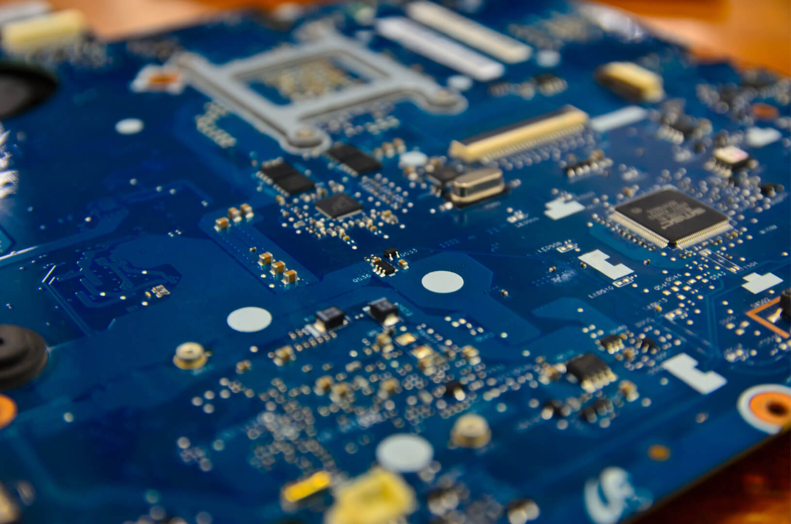
HDI(high-density interconnect) PCBs are advanced circuit boards designed with complex and intricate features that allow for high-density routing and component placement. These boards utilize microvias, fine lines, and small vias to maximize the available space on the board, resulting in reduced size, improved performance, and enhanced functionality. With our state-of-the-art manufacturing facilities and cutting-edge technology, we specialize in producing HDI PCBs that cater to a wide range of applications, including smartphones, tablets, wearables, automotive electronics, and medical devices. Our team of skilled engineers and technicians meticulously design and fabricate HDI PCBs, ensuring the highest levels of precision, reliability, and quality.

By partnering with Bester for your HDI PCB needs, you can expect superior performance, exceptional signal integrity, and improved thermal management. With our commitment to innovation and customer satisfaction, we strive to deliver HDI PCBs that exceed expectations and drive the success of your electronic products. Trust Bester for all your HDI PCB requirements and experience the difference in quality and service that sets us apart from the competition.
A Leading HDI PCB Manufacturer
Over the course of a decade in business, Bester has established a hard-earned reputation for manufacturing PCBs of the highest quality. Our custom PCB manufacturing capabilities enable you to get the finest quality HDI PCBs at competitive prices without min order quantity requirement. Our team run design for manufacture check on your custom PCB file and consult with you to ensure it is ready for manufacturing and that your boards will meet your performance requirements. We also have an on-site quality control department to verify the finished product meet your high quality standards.
- Quality Grade
- Standard IPC 2
- Number of Layers
- 4 – 24layers
- Order Quantity
- 1pc – 10000+pcs
- Build Time
- 2days – 5weeks
- Material
- FR4 standard Tg 140°C,FR4 High Tg 170°C, FR4 and Rogers combined lamination
- Board Size
- Min 6*6mm | Max 457*610mm
- Board Thickness
- 0.4mm – 3.0mm
- Copper Weight (Finished)
- 0.5oz – 2.0oz
- Min Tracing/Spacing
- 2.5mil/2.5mil
- Solder Mask Sides
- As per the file
- Solder Mask Color
- Green, White, Blue, Black, Red, Yellow
- Silkscreen Sides
- As per the file
- Silkscreen Color
- White, Black, Yellow
- Surface Finish
- HASL – Hot Air Solder Leveling, Lead Free HASL – RoHS, ENIG – Electroless Nickle/Immersion Gold – RoHS, Immersion Silver – RoHS, Immersion Tin – RoHS, OSP – Organic Solderability Preservatives – RoHS
- Min Annular Ring
- 4mil, 3mil – laser drill
- Min Drilling Hole Diameter
- 6mil, 4mil – laser drill
- Max Exponents of Blind/Buried Vias
- stacked vias for 3 layers interconnected, staggered vias for 4 layers interconnected
- Other Techniques
- Flex-rigid combination, Via In Pad, Buried Capacitor (only for Prototype PCB total area ≤1m²)
Why Choose Bester

Strong Assembly Capacities
With state-of-the-art facilities and a highly skilled team, we have the capacity to handle even the most complex PCB assembly projects, ensuring your products are manufactured efficiently and accurately.

Quality Assurance
Our rigorous quality control processes and extensive testing procedures guarantee that every PCB assembly we produce meets the highest industry standards for reliability and performance, giving you peace of mind and confidence in our services.

One-stop Service
From PCB fabrication and design to component sourcing and IC programming, Bester offers a comprehensive range of services under one roof, streamlining the production process and saving you time and effort.

Fast Turnaround
Our commitment to fast turnaround times means that your PCB assembly projects will be completed on schedule, allowing you to meet your production deadlines and get your products to market quickly.
Clients and Certifications

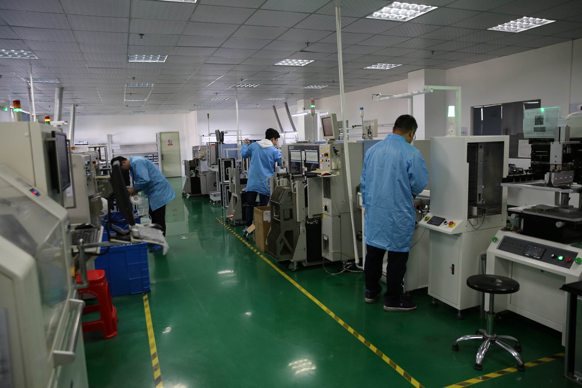
Electronics Manufacturing Capabilities at Bester
Manufacturing Capabilities
- 100% ESD Components Control
- 8 SMT Lines
- 4 DIP Lines
- 40 Automatic Robotic Soldering
- CNC Machining
- Automated Conformal Coating
- Injection Molding
- 3D Printing
Certifications
- ISO 9001
- UL
- SGS
- IPC
- RoHS
- CE
- FCC
- SRDI (China’s “Specialized, Refinement, Differential, Innovation” Enterprise)
- HNTE (China’s High and New Technology Enterprise)
Industries We Serve

Automotive
We understand the critical role that PCBA plays in the automotive industry. With our comprehensive PCBA services, we cater to the specific needs of automotive manufacturers, helping them deliver reliable and high-performing electronic systems.
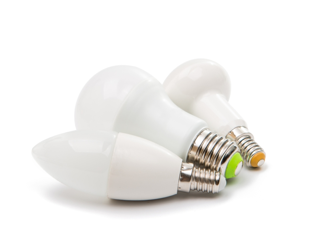
LED
In the LED market, Bester provides top-notch PCBA solutions that are essential for the production of high-quality LED lighting products. We work closely with LED manufacturers to ensure that their PCBAs meet the stringent requirements of energy efficiency, durability, and performance.
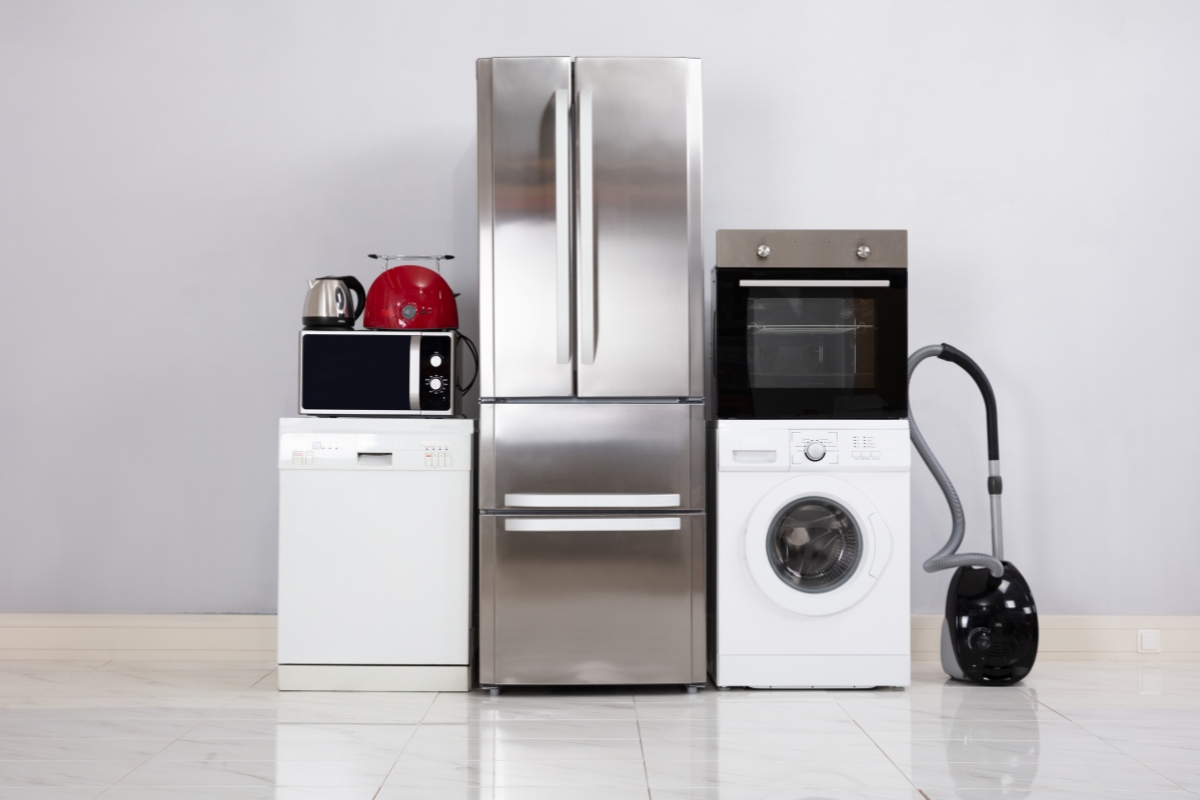
Consumer Electronics
Bester caters to the consumer electronics market by offering a wide range of PCBA services that enable the production of innovative and user-friendly electronic devices. We collaborate with consumer electronics manufacturers to ensure that their PCBAs meet the highest standards of quality and functionality.

Industrial
In the industrial sector, Bester’s PCBA services play a crucial role in the development of reliable and efficient electronic systems. We work closely with industrial equipment manufacturers to meet their specific requirements, ensuring that our PCBAs can withstand harsh environmental conditions and deliver optimal performance.
PCBA APPLICATIONS
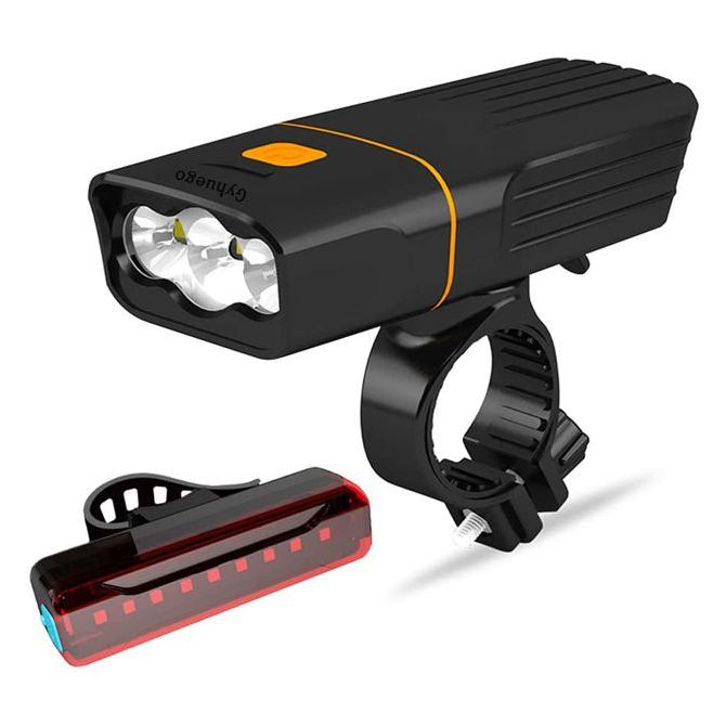
Bike Light PCBA
PIR Motion Sensor PCBA
LED PCBA

Ready to Start Your PCB Assembly Projects?