PCB Fabrication
Transforming Your Vision into Reality: Unleash the Power of Customized PCB Fabrication with Bester!
PCB Fabrication
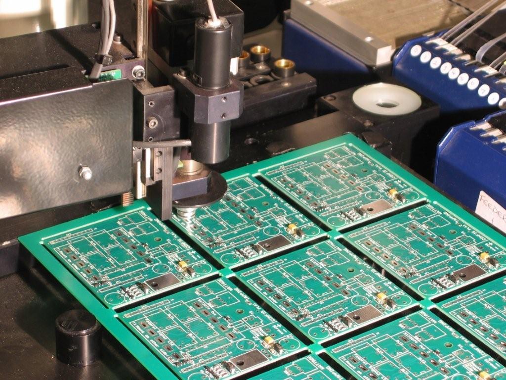
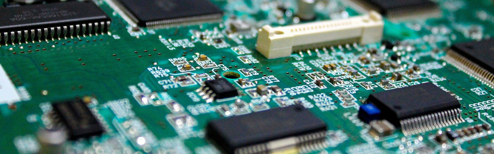
PCB fabrication is a crucial step in the manufacturing process of electronic devices. It involves the creation of a custom-designed circuit board that serves as the foundation for various electronic components. The process begins with the design phase, where the layout and specifications of the circuit board are determined. Once the design is finalized, it is transferred onto a copper-clad laminate material, which acts as the base for the PCB. The next step is to etch away the excess copper, leaving behind the desired circuitry pattern. This is achieved through a combination of chemical etching and photoengraving techniques. After the etching process, the board undergoes a thorough cleaning to remove any leftover residue and contaminants. The next crucial step is drilling, where holes are created for component placement and electrical connections. The holes are then plated to ensure a secure connection. Once the drilling and plating are complete, a solder mask is applied to protect the circuitry and provide insulation. Finally, a silkscreen layer is added, which includes component labels, logos, and other identification markings. PCB fabrication requires precision and expertise to ensure the highest quality and functionality of the circuit board.

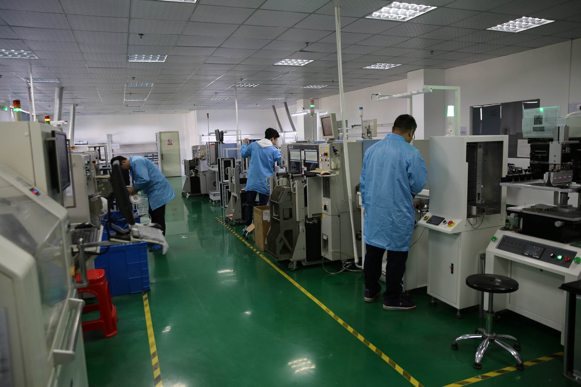
At Bester, we are proud to offer top-notch PCB fabrication services to our valued customers. With years of experience and expertise in the field, we are committed to delivering high-quality printed circuit boards that meet the unique requirements and specifications of our clients. Our state-of-the-art manufacturing facility is equipped with advanced technology and cutting-edge machinery that enables us to produce PCBs with precision and accuracy. We have a team of skilled engineers and technicians who work diligently to ensure that every step of the fabrication process is carefully executed, from the initial design to the final production. With a strong focus on quality control, we implement rigorous testing procedures to guarantee the reliability and functionality of each PCB we manufacture. Whether it’s a small-scale project or a large-scale production run, we have the capacity and capability to handle any order size.
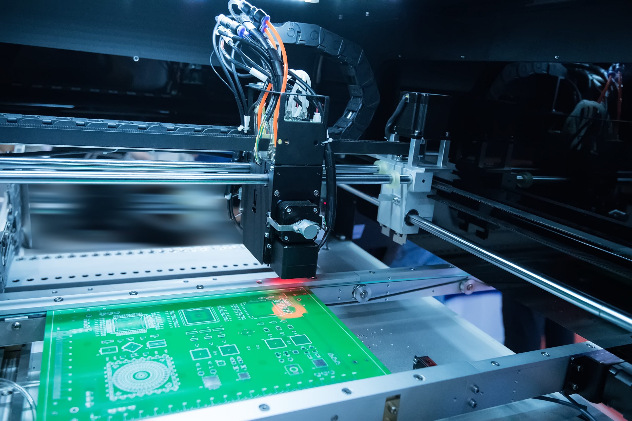
PCB Fabrication Process
There is no such thing as a standard printed circuit board. Each PCB has a unique function for a particular product. Therefore, producing a PCB is a complex process of many steps. This overview covers the most important steps when producing a multilayer PCB. When you order PCBs from Bester Tech, you are buying quality that pays for itself over time. This is guaranteed through a product specification and quality control that is far more stringent than other suppliers, and ensures that the product delivers what it promises. In the production flow below you can see where the process is unique or goes beyond the IPC standard.
Pre Production
We use the data (Gerber file) you provide to create the production information for your customized boards. Our experts match your specifications with the capacities for compliance purposes.
Inner Layer Imaging
When making circuit board, the imaging process is what defines the circuit traces. Traditional imaging process needs a UV-light and photo-tool to transfer images, while LDI only uses a computer-controlled, highly focused, laser beam to directly define the circuit pattern onto the board.
Inner Layer Etching
Leverage the etching process to eliminate any undesirable copper residues from the panel. After removal, we remove the dry film to remain with copper circuitry as well, which is in line with the PCB design.
Inner Layer AOI
Inspection of the circuitry against digital images to verify that the circuitry matches the design and that it is free from defects. Achieved through scanning of the board and then trained inspectors will verify any anomalies that the scanning process has highlighted.
Lamination
Apply an oxide layer to the inner board layers and then stack them together using prepreg to create insulation between them. Copper foil is added to the upper and lower stack parts.
PCB Drilling
Bore the holes that will later act as electrical contacts in the multilayer board. Drilling is a mechanical process that PCB manufacturers optimize to obtain registration to the internal layer links.
Electroless Copper Deposition
Apply thin copper layer deposits on the holes that drilled earlier on the walls. PTH offers copper deposits, which conceal the hole walls and the whole panel.
Outer Layer Imaging
Outer layer imaging resembles the internal layering process. However, in outer layer drilling, get rid of the dry film and maintain the circuitry. Then plate the extra copper later in a clean environment.
Graphic Plating
The second electrolytic plating process, where we carry out extra plating in dry film parts (circuitry). After depositing the copper, we should apply tin to prevent the plated copper from oxidation.
Outer Layer Etching
Take out the dry blue film and scrape all the unwanted copper residues. The tin deposits resist the etching process to protect the copper deposit, then chemically eliminated the tin residues to leave behind the circuitry.
Solder Mask
With the help of artwork and Ultraviolet light, expose some PCB parts and remove all the exposed parts. Then completely cure the remaining solder mask to create a quality finish.
Surface Finish
Surface finish can maintain the exposed copper circuitry meanwhile provide a solderable surface when soldering components to the PCB. Metallic and organic are the two main kinds of surface finishes.
Electrical Test
Test all boards before shipping to ensure all of the printed circuit boards are free of defects and meet the standards you expect. Test including flying probe, fixtureless testers. And we also have universal grid testing capability. These machines use fixtures built specifically for your PCB.
Profiling
Route the PCB production panels into particular sizes and shapes according to the production file. PCB V-Scoring is a process of cutting a ‘V’ shaped groove at the top and bottom of a printed circuit board, leaving a thin layer between the Vees. Once we have done this, it can easily separate the PCB Board at the V by applying minimal pressure.
Final Visual Inspection
A team of sharp-eyed individuals scrutinizes each product. The process involves visually examining the board in line with the set standards.
Rapid PCB Prototyping and Small-volume Production
Our state-of-the-art assembly equipment enables us to meet all your PCBA needs under one roof in an inexpensive way, our Printed Circuits Boards Assembly Capability includes but not limited to what are listed below, as we are updating our equipment constantly to keep us on the cutting edge.
- Circuit Board Specifications
- Maximum Panel size: 19.7″ x 31.5″, Maximum Number of Layers: 1-40, Copper Thickness: 0.5 oz to 5.0 oz, Minimum Line Width: 3 mil, Minimum Line spacing: 3 mil, Smallest Hole: 0.006″, Blind, Buried and plugged Vias, Controlled impedance
- Material
- Thickness: 0.008″ to 0.240″, FR-4, High TG FR-4, PTFE, Aluminum Base, Rogers, Specialized material per your request
- Solder Mask
- LPI – Green, Yellow, Black, Red, Blue, White, etc. (Inquire for more options), Peelable Mask
- Final Finishes
- SMOBC (HASL), Carbon, Selective Gold Plating, Hard and Soft Gold, Immersion Gold, Immersion Silver, Immersion Tin, OSP
- Legend
- White, Yellow, Black (Inquire for more options)
- Inspection Methods
- 100% Visual inspection, Electrical testing – Flying probe or Nails Bed, Sample lot inspection, Cross sectioning
- Delivery
- Rush: 24 Hours, Standard Prototype: 5 days, Standard Production: 10 days
Why Choose Bester

Strong Assembly Capacities
With state-of-the-art facilities and a highly skilled team, we have the capacity to handle even the most complex PCB assembly projects, ensuring your products are manufactured efficiently and accurately.

Quality Assurance
Our rigorous quality control processes and extensive testing procedures guarantee that every PCB assembly we produce meets the highest industry standards for reliability and performance, giving you peace of mind and confidence in our services.

One-stop Service
From PCB fabrication and design to component sourcing and IC programming, Bester offers a comprehensive range of services under one roof, streamlining the production process and saving you time and effort.

Fast Turnaround
Our commitment to fast turnaround times means that your PCB assembly projects will be completed on schedule, allowing you to meet your production deadlines and get your products to market quickly.
Clients and Certifications

Electronics Manufacturing Capabilities at Bester
Manufacturing Capabilities
- 100% ESD Components Control
- 8 SMT Lines
- 4 DIP Lines
- 40 Automatic Robotic Soldering
- CNC Machining
- Automated Conformal Coating
- Injection Molding
- 3D Printing
Certifications
- ISO 9001
- UL
- SGS
- IPC
- RoHS
- CE
- FCC
- SRDI (China’s “Specialized, Refinement, Differential, Innovation” Enterprise)
- HNTE (China’s High and New Technology Enterprise)
Industries We Serve

Automotive
We understand the critical role that PCBA plays in the automotive industry. With our comprehensive PCBA services, we cater to the specific needs of automotive manufacturers, helping them deliver reliable and high-performing electronic systems.
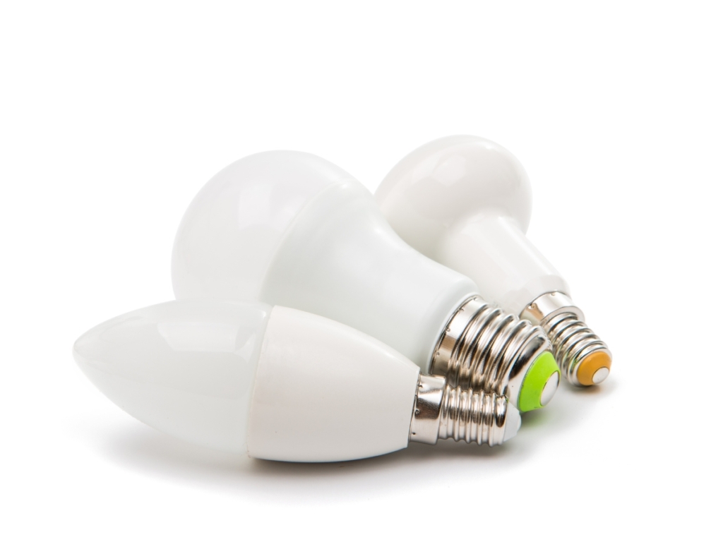
LED
In the LED market, Bester provides top-notch PCBA solutions that are essential for the production of high-quality LED lighting products. We work closely with LED manufacturers to ensure that their PCBAs meet the stringent requirements of energy efficiency, durability, and performance.
Consumer Electronics
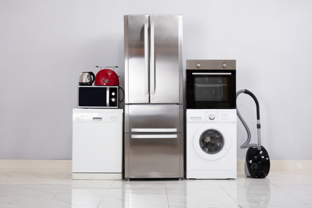
Bester caters to the consumer electronics market by offering a wide range of PCBA services that enable the production of innovative and user-friendly electronic devices. We collaborate with consumer electronics manufacturers to ensure that their PCBAs meet the highest standards of quality and functionality.

Industrial
In the industrial sector, Bester’s PCBA services play a crucial role in the development of reliable and efficient electronic systems. We work closely with industrial equipment manufacturers to meet their specific requirements, ensuring that our PCBAs can withstand harsh environmental conditions and deliver optimal performance.
PCBA APPLICATIONS
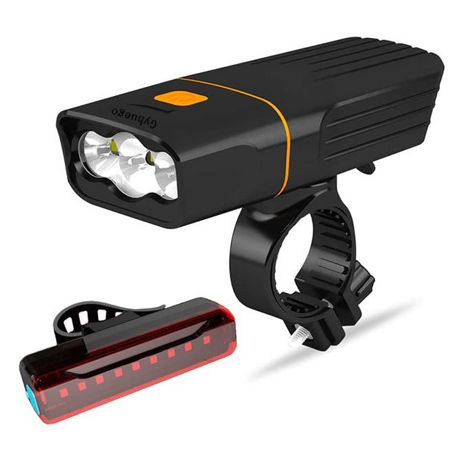
Bike Light PCBA
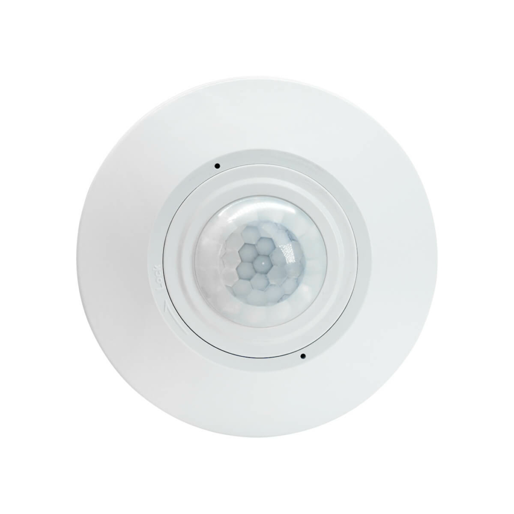
PIR Motion Sensor PCBA
LED PCBA
PCB Manufacturing FAQ
How to Get Quotation of Standard PCBs
Free PCB quotation is just a click or one call away. Send us an email or give us a call for the quickest quotation.
Advantages to PCB With Bester
Bester is a full-service turnkey PCB solution that can handle everything from prototype to fabrication to assembly. We have been fabricating high-quality standard PCB for over ten years and are fully compliant with ISO9001:2015 quality standards. All of our standard PCBs are IPC2 compliant, and we do strict internal quality assurance testing to ensure the board that arrives at your facility is one you know you can rely on.
We offer PCB solutions that fit your budget. You can order just a few prototype boards to test your design, and then place a bulk order for your standard PCBs to save even more money. We’ll give you a free instant quote so you’ll know just want to expect and so that you can plan accordingly. We also offer complete technical support from PCB experts. Call us up, chat online or email us with any questions, whichever is the most convenient for you. We’ll handle your concerns or questions as quickly as possible. We have obtained over 99 percent customer satisfaction rate, and as soon as you start ordering printed circuit boards.

Ready to Start Your PCB Assembly Projects?