The Rorschach Test of Manufacturing

When you look at a grayscale X-ray image of a Ball Grid Array (BGA) for the first time, your instinct is usually alarm. You see a dark circle (the solder ball) riddled with lighter, irregular blotches. It looks like a disease, a sponge, or—to the uninitiated—a defect that needs to be purged.
In the inspection room, however, we don’t inspect for aesthetics; we inspect for physics. Those lighter blotches are voids—pockets of gas trapped during the reflow process. They are ugly, yes. But in the vast majority of cases, they are structurally benign.
The challenge in modern electronics manufacturing isn’t achieving a “perfect” void-free solder joint, which is a prohibitively expensive and often damaging pursuit. The challenge is distinguishing between the cosmetic void that will survive ten years in the field and the structural void that will crack under thermal stress. To do that, we have to ignore the gut reaction to “ugly” images and rely entirely on the area ratios defined in IPC-A-610.
The 25% Rule
The industry standard for electronic assembly acceptability, IPC-A-610, is surprisingly forgiving when it comes to voiding. Whether you are building a Class 2 product (laptops, industrial controls) or a Class 3 product (life support, aerospace), the criteria for BGA voiding are often identical. Per IPC-A-610 and its companion J-STD-001, a solder ball is acceptable provided the cumulative void area does not exceed 25% of the total ball area.
That number usually shocks people. A 25% void looks massive on a monitor—like a quarter of the connection is missing. But the physics tell a different story. Solder paste, particularly standard SAC305 lead-free alloys, contains flux volatiles that must outgas during reflow. If the time above liquidus is short, or if the component is heavy, some gas gets trapped. This is natural. The remaining 75% of the solder volume is more than sufficient to carry the electrical current and withstand mechanical shock.
In fact, internal studies and industry reliability data show that BGA balls with 15–20% voiding often survive just as many thermal cycles as those with 1% voiding.
There is a movement, often pushed by high-end niche manufacturers, suggesting that any void is a failure. You might hear arguments for vacuum reflow ovens, which pull the atmosphere out of the chamber during soldering to collapse bubbles. If you are building for a deep-space satellite where repair is impossible, vacuum reflow is a valid, albeit expensive, requirement. For the other 99% of electronics, chasing zero voids is a waste of money and thermal budget. Subjecting a board to multiple rework heat cycles to fix a compliant 15% void does more damage to the laminate and copper pads than the void ever would.
The Geometry of Acceptance
Inspection is a geometric calculation, not a vibe check. When an Automated X-ray Inspection (AXI) machine or a human operator reviews a BGA, the task is to calculate the projected area of the voids relative to the projected area of the ball. It is a simple ratio: (Sum of Void Areas) / (Total Ball Area). If the ball is 20 mils in diameter, we are measuring the pixel count of the light spots versus the dark circle.
However, voids are rarely perfect circles. They often appear as “Swiss cheese”—clusters of tiny bubbles merging and separating. Calculating the exact area of these irregular shapes is an estimation, even for advanced algorithms. The machine draws a perimeter around the void clusters and sums them up.
When the result hovers right at the limit—say, 24% or 26%—human judgment becomes critical. We have to look at image fidelity. Is that a single large void, or a cluster of small ones? The standard allows for cumulative calculation, meaning lots of tiny bubbles count the same as one big one, provided they don’t violate other rules about location.
The Thermal Pad Exception (QFN/BTC)

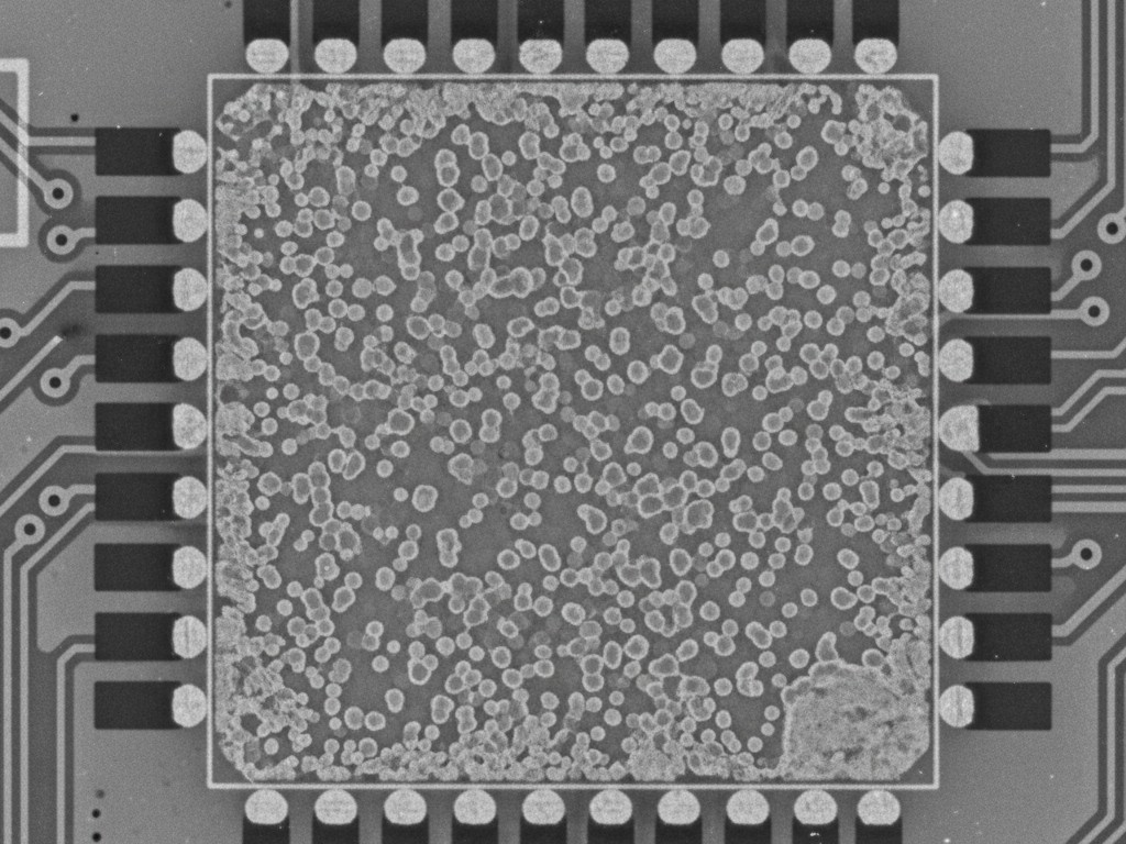
Criteria shift drastically when we move away from signal pins (BGAs) to thermal pads. Components like QFNs (Quad Flat No-leads) and other Bottom Termination Components (BTCs) have a large exposed pad in the center primarily for heat dissipation, not electrical signal. Because it is a large, flat surface soldered to a matching large, flat pad on the PCB, outgassing has nowhere to go. Think of it like flattening pizza dough without trapping any air bubbles; it’s nearly impossible.
Consequently, the IPC limit for these thermal pads is significantly higher, typically allowing up to 50% voiding. Engineers often panic when they see a QFN thermal pad that looks like a honeycomb, flagging it as a reject. But if that pad is 50% soldered, the thermal transfer efficiency is usually sufficient for the component’s rating. While datasheets from manufacturers like TI or Analog Devices sometimes specify stricter limits for high-power RF applications, 50% is the standard for general digital logic.
If you are consistently seeing massive voids in these thermal pads—say, 60% or higher—the issue is rarely the reflow profile. It is almost always the stencil design. A 1:1 aperture opening (where the hole in the stencil is the same size as the pad) deposits too much paste, trapping volatiles in the center. The fix is not to tweak the oven, but to use a “window-pane” stencil design. Breaking the large square into smaller panes with channels allows gas to escape, often dropping voiding from 60% to 15% overnight.
Location is the Real Killer

While the size of the void gets all the attention, the location is what keeps quality engineers awake at night. A large “bulk void” floating benignly in the center of a solder ball is rarely a reliability threat because it is surrounded by solid metal. The dangerous voids are the ones that touch the interface—the boundary between the solder and the component pad, or the solder and the PCB pad.
We call these “Champagne voids” because they gather at the interface like bubbles in a glass. Even if these voids only account for 5% of the area, they can be catastrophic. They create a stress concentration point right where the intermetallic compound (IMC) forms. Under drop shock or vibration, a crack can initiate at that void and propagate across the pad, severing the connection. A 5% interface void is infinitely worse than a 20% bulk void. This is why automated pass/fail numbers can be deceiving; a machine might pass a board with 5% voiding that a human eye would reject because that 5% is sitting right on the pad surface.
This is also where confusion often arises regarding “Head-in-Pillow” (HiP) defects. You might see a shape that looks like a void or a weird double-circle on the X-ray, but HiP isn’t a void at all. It is an open circuit where the ball has deformed but not coalesced with the paste—looking like a snowman or a head resting on a pillow. Unlike a void, which is a process indicator, HiP is a functional failure. Do not let the terminology confuse you; if you have HiP, you have an open, not a voiding problem.
The False Positive Trap

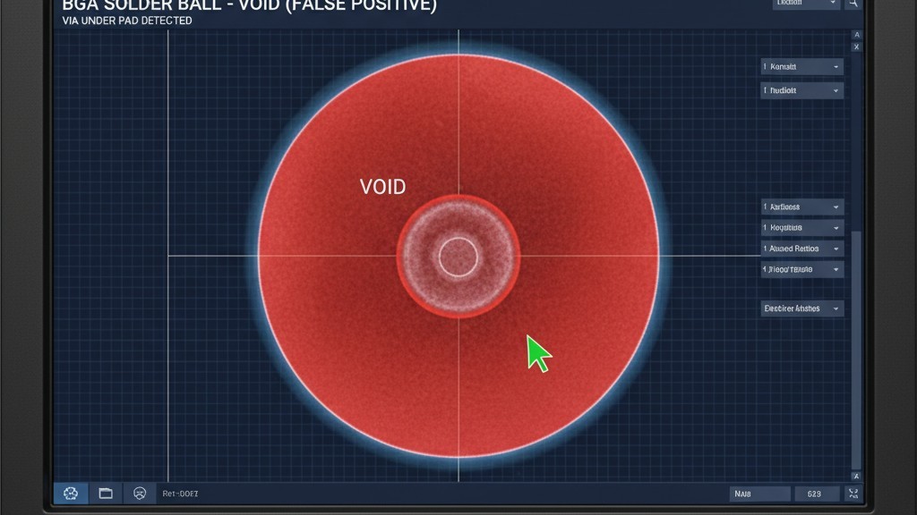
Modern X-ray machines are incredible, but they are not omniscient. They struggle with background noise. If you have a via (a plated hole) located directly under a BGA pad, the X-ray sees the air inside the via barrel and flags it as a void in the solder ball. This is a classic false positive where the software sees a density change and screams “Defect!”
We review these “bone piles” of rejected images daily. In many cases, what the machine flagged as a 30% void is actually a perfectly soldered ball sitting on top of a tented via. We have to verify the location of the via in the design files to confirm. If we blindly accepted the machine’s judgment, we would be scrapping or reworking perfectly good hardware.
Reliability Over Perfection
The goal of inspection is reliability, not geometric perfection. By adhering to the IPC Class 2 and 3 limits—25% for signal balls, 50% for thermal pads—and focusing our scrutiny on dangerous interface voids rather than benign bulk voids, we protect the product without destroying the yield. We accept that solder is a dynamic, organic material that outgasses and moves. As long as the numbers and the physics align, the board ships.


