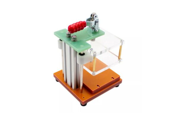
The pressure to catch manufacturing faults before boards ship is non-negotiable. A single escaped defect in a critical system can cost exponentially more than the testing that would have caught it. This reality drives many engineering teams toward in-circuit testing (ICT) as the default, a method long considered the gold standard for coverage. Full ICT offers comprehensive access to nearly every node on a board, promising fault detection rates that approach the theoretical maximum. For high-volume production, the investment makes sense; the fixed costs of fixture engineering and test equipment amortize across thousands of units, driving the per-unit burden down to negligible levels.
But the economics flip when production volumes drop. For runs below a few hundred units, the very strengths of ICT become liabilities. The custom fixture required for each board design carries a steep, fixed engineering cost that doesn’t scale. Lead times stretch as fixtures are designed, built, and debugged. Design iterations, common in new product introduction, invalidate fixtures entirely, forcing the cycle to restart. At Bester PCBA, we have watched this math play out across hundreds of projects. For runs below 200 to 300 units, full ICT rarely earns its keep.
The alternative is not to abandon rigorous testing, but to replace the fixture-dependent model with a leaner, faster strategy built on boundary scan, vectorless testing, and focused functional test. This combination delivers comparable fault coverage, eliminates the fixture bottleneck, and provides a faster debug loop when faults are found. This shift isn’t ideological; it’s a practical response to the mathematical and mechanical friction that ICT imposes on low-volume, agile production.
The ICT Assumption and Where It Breaks
In-circuit testing became the industry standard in an era of high-volume, stable designs. The model was simple: invest heavily upfront in a custom test fixture and a sophisticated tester, then leverage that investment across tens of thousands of identical units. With per-unit test times measured in seconds, the marginal cost per board was effectively zero after the fixed costs were absorbed. For a consumer electronics manufacturer running 50,000 units of the same SKU, the math was unassailable.
That production model has fractured. Modern electronics manufacturing increasingly serves markets with high mix and low volume. Product lifecycles are shorter, design iterations are more frequent, and customization is a competitive advantage. A company might produce 150 units of one variant, iterate the design, then produce 200 of the next. The assumption that a single fixture will test thousands of identical boards no longer holds. The fixed costs that were negligible in high volumes become punishing when spread over a few hundred units.
The model breaks where the total cost of ICT infrastructure exceeds the risk-adjusted cost of alternative strategies. That threshold isn’t arbitrary. It is a function of fixture cost, engineering time, production lead time, and the coverage achievable through fixtureless methods. For most board designs, that threshold sits between 200 and 300 units.
The Fixed Cost Trap of In-Circuit Testing
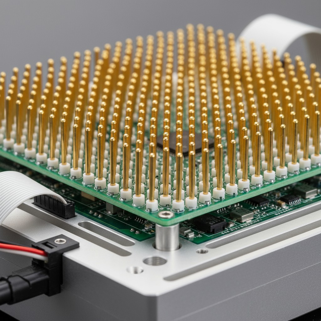
While the fixture is the most visible cost of ICT, the true economic burden is far broader. A custom ICT fixture is not an off-the-shelf purchase; it is an engineered artifact, purpose-built for a specific board layout. The design process requires translating the board’s netlist and component placement into a mechanical structure studded with spring-loaded test probes, each aligned to a specific test point with sub-millimeter precision. The fixture must account for component tolerances, board warpage, and probe wear. It must then be validated and debugged—a process that often reveals unforeseen issues with probe access or signal integrity.
Fixture Engineering Costs and Lead Times
The engineering cost for a moderately complex fixture typically falls between $8,000 and $15,000. High-density boards with fine-pitch components or limited test point access can push that figure to $25,000 or more. This is purely the cost of the custom mechanical and electrical interface needed to connect the board to the ICT equipment, separate from the capital expense of the tester itself.
The lead time is equally consequential. From the moment a board design is finalized, fixture design and fabrication typically require two to four weeks, extending to six for complex designs. During this period, production is stalled. Boards may be assembled, but they cannot be tested. They sit in inventory, waiting. If the design changes during this window—a common occurrence in new product introduction—the fixture must be revised or scrapped. The clock resets.
The Breakeven Math for Low-Volume Runs
The economic trap becomes clear when fixture costs are divided by unit count. A $12,000 fixture for a 100-unit run adds a $120 burden to each board. For a board with a $500 bill of materials, that’s a 24 percent testing overhead. Even if the ICT process is fast, the economic efficiency is poor. That same fixture amortized over 500 units drops the per-unit cost to $24, a far more acceptable five percent overhead. The difference is purely a function of volume.
The breakeven point is where the total cost of ICT—including engineering, setup, and the opportunity cost of lead time—equals the cost of a fixtureless alternative. For a strategy combining boundary scan, vectorless testing, and a lean functional test, the infrastructure cost is dramatically lower. Boundary scan requires no fixture, and vectorless testing uses reusable sensors that work without mechanical contact. Any functional test fixture is typically minimal and generic, not a board-specific artifact requiring weeks of engineering.
At production volumes below 200 units, the economics of ICT collapse. Below 300 units, the case is marginal, dependent on board complexity. Only above 300 units for stable, non-iterative designs does ICT begin to make clear economic sense again.
What Boundary Scan and Vectorless Testing Actually Are
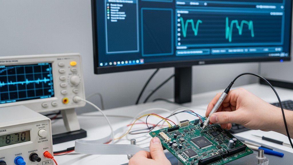
The alternative to fixture-based testing is not a compromise in rigor but a shift to methods that leverage existing design infrastructure and non-contact measurement. These tools were developed to address the same trend that undermines ICT: increasing board density and shrinking access to physical test points.
Boundary scan, formalized in the IEEE 1149.1 standard (commonly known as JTAG), embeds test logic directly into a board’s integrated circuits. Compliant chips include a chain of cells at each input and output pin. During a test, a simple four-wire interface shifts patterns into these cells, controlling the logic states on the board’s nets. The resulting states are captured and shifted out for analysis, allowing the tester to control and observe signals at the pin level without physical contact. This non-invasive method is highly effective at detecting shorts, opens, and stuck-at faults between compliant devices.
Vectorless testing complements this by using capacitive and inductive measurements to detect faults across the entire board. A sensor array positioned near the board measures the electromagnetic signature of assembled components and traces. Shorts create measurable capacitive coupling; opens show characteristic impedance changes. The method is fast, non-contact, and can infer component presence, polarity, and approximate value, making it effective at catching gross manufacturing defects like missing components, reversed diodes, or bridged traces.
Coverage Comparison: The Numbers Behind the Trade-Off
The primary objection to abandoning ICT is coverage. While ICT can, in principle, access every node on a board with enough test points, the claim that alternatives are inferior is incomplete. The real question is whether they achieve sufficient coverage to catch the faults that actually occur, and if a focused functional test can close the remaining gap.
What Boundary Scan Covers
Boundary scan coverage depends on how many components on the board are compliant with the JTAG standard. For boards dominated by digital logic—microprocessors, FPGAs, memory—coverage is extensive. The scan chain can test the interconnect between these devices with fault detection rates exceeding 95 percent for shorts, opens, and stuck-at faults. A board where 80 percent of components are compliant will achieve roughly 70 to 85 percent net coverage. Analog sections, discrete components, and legacy parts are invisible to this method. However, for digital-heavy designs, boundary scan alone delivers coverage comparable to ICT for the interconnect layer, where most assembly faults occur.
What Vectorless Testing Adds
Vectorless testing fills the gaps left by boundary scan, particularly for passive components and gross assembly defects. Capacitive measurements can detect missing resistors, incorrect capacitor values, and reversed diodes. While less precise than ICT’s direct measurements, it is an effective screen for the most common errors: wrong component, missing component, or severe misalignment. This adds another 10 to 20 percent to the total fault coverage, providing a non-contact verification layer for parts that boundary scan cannot see.
The Remaining Gap and How Lean Functional Test Closes It
The combination of boundary scan and vectorless testing still leaves a gap in functional validation and analog performance. A component can be present and connected correctly but still fail to operate within specification. A power supply might deliver voltage but with excessive ripple. This is where a lean functional circuit test (FCT) plays its role. Unlike a full ICT setup, a lean FCT validates that the board performs its intended function under realistic conditions. It applies power, stimulates inputs, and measures outputs. For a motor controller, it might verify PWM signal generation; for a communication board, it might check for error-free data transmission. The functional test complements the structural tests, catching faults the other methods cannot see.
Combined, these three methods typically achieve 85 to 95 percent fault coverage. This isn’t 100 percent, but neither is ICT in practice. Due to test point limitations and probe wear, real-world ICT coverage often falls short of its theoretical maximum. The difference in coverage is far smaller than the penalty in cost and lead time.
The Debug Loop Advantage
Test coverage is only half the value equation; the other is the speed and precision of fault isolation. A test that detects a fault but provides vague diagnostics increases the time and cost required to find the root cause.
While ICT is great at flagging faults, its diagnostics can be frustratingly vague. A tester might report that node 47 is shorted to ground, but it doesn’t explain why or where. The technician must trace the schematic, locate the net, and visually inspect the area—a process that can consume hours on a dense, multi-layer board.
Boundary scan diagnostics are fundamentally different. Because the scan chain is embedded in the components, the test isolates faults to specific pins and devices. A short between two nets is identified by the exact device pins involved, narrowing the search to a few square millimeters. Opens are detected between specific driver and receiver pairs. The diagnostic output is not a fault code. It is a map. This precision means a fault that takes an hour to debug with ICT data can often be resolved in 10 to 20 minutes with boundary scan. For a 100-unit run with a typical defect rate, the cumulative debug time saved can exceed 10 hours.
Lead Time and Flexibility: The Hidden Value
The economic argument against ICT for low volumes is compelling, but the lead time penalty is just as significant. The two-to-four-week fixture engineering process imposes a mandatory delay between design freeze and test readiness. For new product introduction, where time to market is critical, this delay is often unacceptable.
Boundary scan and vectorless testing eliminate this wait. The test setup can be configured in hours or days, not weeks, allowing boards to move from assembly to test to shipment in a continuous flow. This flexibility is crucial when designs iterate. An early prototype run might reveal issues requiring board layout changes. With ICT, every revision demands a new or reworked fixture, incurring the cost and lead time all over again. Boundary scan test patterns, generated from the netlist, update automatically with the design. This creates a test strategy that supports iterative development rather than penalizing it.
When to Still Choose ICT
But the case against low-volume ICT isn’t absolute. Certain designs and production contexts still justify the investment.
Boards with high-density analog or RF sections are poor candidates for a purely fixtureless strategy. Analog components lack boundary scan logic, and critical performance characteristics like gain or phase noise cannot be verified structurally. If analog or RF circuitry represents more than 40 percent of the board’s functionality, the case for ICT strengthens considerably.
Compliance-driven industries like medical, aerospace, and automotive often operate under regulations that mandate specific test coverage or methods. If a governing standard requires in-circuit testing or equivalent node-level access, alternative strategies may not suffice. Here, the cost of ICT is a non-negotiable cost of market entry.
Finally, a clear and committed path to high-volume production changes the math. If an initial 150-unit run is expected to scale to 1,000 units within six months, the fixture cost amortizes across the total anticipated volume. This requires high confidence in the forecast and a stable design, but it can make the upfront investment worthwhile.
Building the Alternative Test Strategy
Replacing ICT is not a simple swap; it’s a reconfiguration of the test architecture into a layered strategy, where each layer catches faults the others might miss.
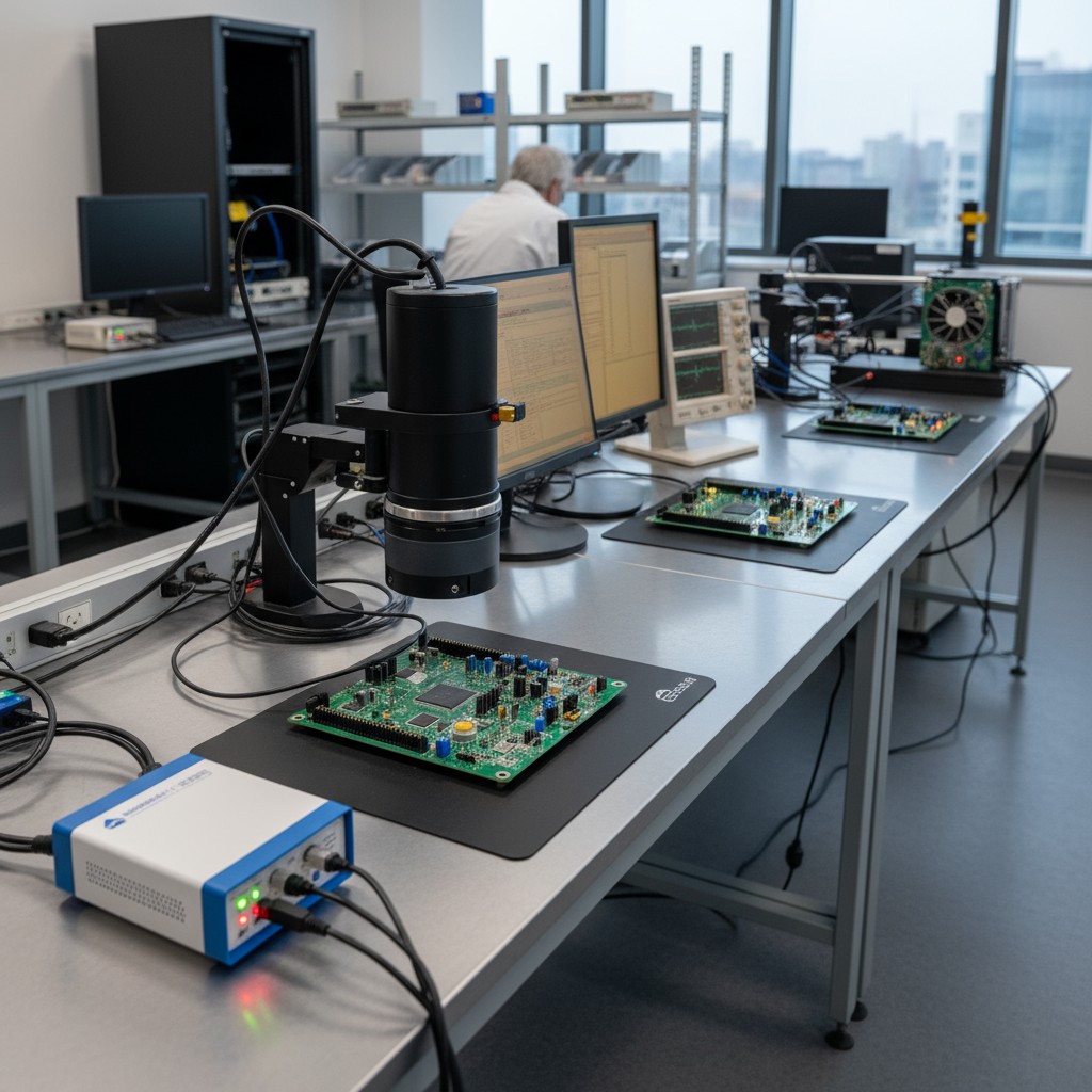
The process should be sequential. The first layer is boundary scan, which runs quickly on all compliant devices to catch interconnect faults on the digital portions of the board. Boards that fail are flagged for immediate rework, preventing catastrophic failures when power is applied later. The second layer is vectorless testing, which runs across the entire board to detect missing or incorrect passive components, gross shorts, and polarity errors. It covers the components and nets invisible to the scan chain.
The third and final layer is a focused functional test. With structural faults already filtered out, the board is powered on to validate its critical functions under realistic operating conditions. The scope is tailored to the board’s purpose—verifying ADC accuracy on a data acquisition board or load regulation on a power supply. This sequence ensures that catastrophic faults are caught early and non-destructively, minimizing debug time on the more complex functional failures.
For boards with hybrid complexity—a dense digital core surrounded by analog signal conditioning, for instance—a hybrid strategy may be best. A partial ICT fixture can be designed to probe only the critical analog section, leaving the digital portion to boundary scan. The economics of a partial fixture are more favorable, reducing cost and lead time while still delivering the necessary coverage for the entire design.


