In CAD, a castellated module looks like the perfect integration strategy. It drops onto the mainboard like a Lego brick, flat and secure, offering pre-certified wireless or compute power without the headache of RF layout. It feels solid. But that visual simplicity is a trap. Once the board leaves the reflow oven and enters the thermal reality of the field, that “solid” module becomes a rigid, ceramic-heavy island fighting against a flexible FR4 sea.
The only thing mediating this fight is a series of tiny solder joints along the edge. If you treat these joints as mechanical fasteners, the design will fail. Solder is a brittle alloy, not a structural adhesive. It fatigues under shear stress, cracks under vibration, and fractures when the board flexes. The failure rarely happens on the bench. It happens six months later, when a fleet of tracking units in Minnesota goes dark during a cold snap, or a drone lands too hard on concrete. The difference between a reliable product and a recall often comes down to tenths of a millimeter in pad geometry that most datasheets explicitly tell you to ignore.
The Physics of the Corner Crack
The primary enemy inside the joint is the Coefficient of Thermal Expansion (CTE) mismatch. Most high-performance modules—whether it’s a u-blox GPS receiver or a dense cellular modem—are built on substrates that are mechanically stiffer and thermally distinct from the standard FR4 of your carrier board. When the device powers up, or when ambient temperature swings from -40°C to +85°C, the mainboard and the module expand at different rates.

This expansion creates a shear force that rips at the solder joints. The stress isn’t distributed evenly; basic mechanics dictates it concentrates at the points furthest from the center: the corners. The corner pads are the fulcrums of the assembly, taking the brunt of every thermal cycle and mechanical twist. If you examine a failed board under a microscope, you will almost invariably see the hairline fracture starting at the toe of a corner pad, propagating through the intermetallic layer until the electrical connection severs.
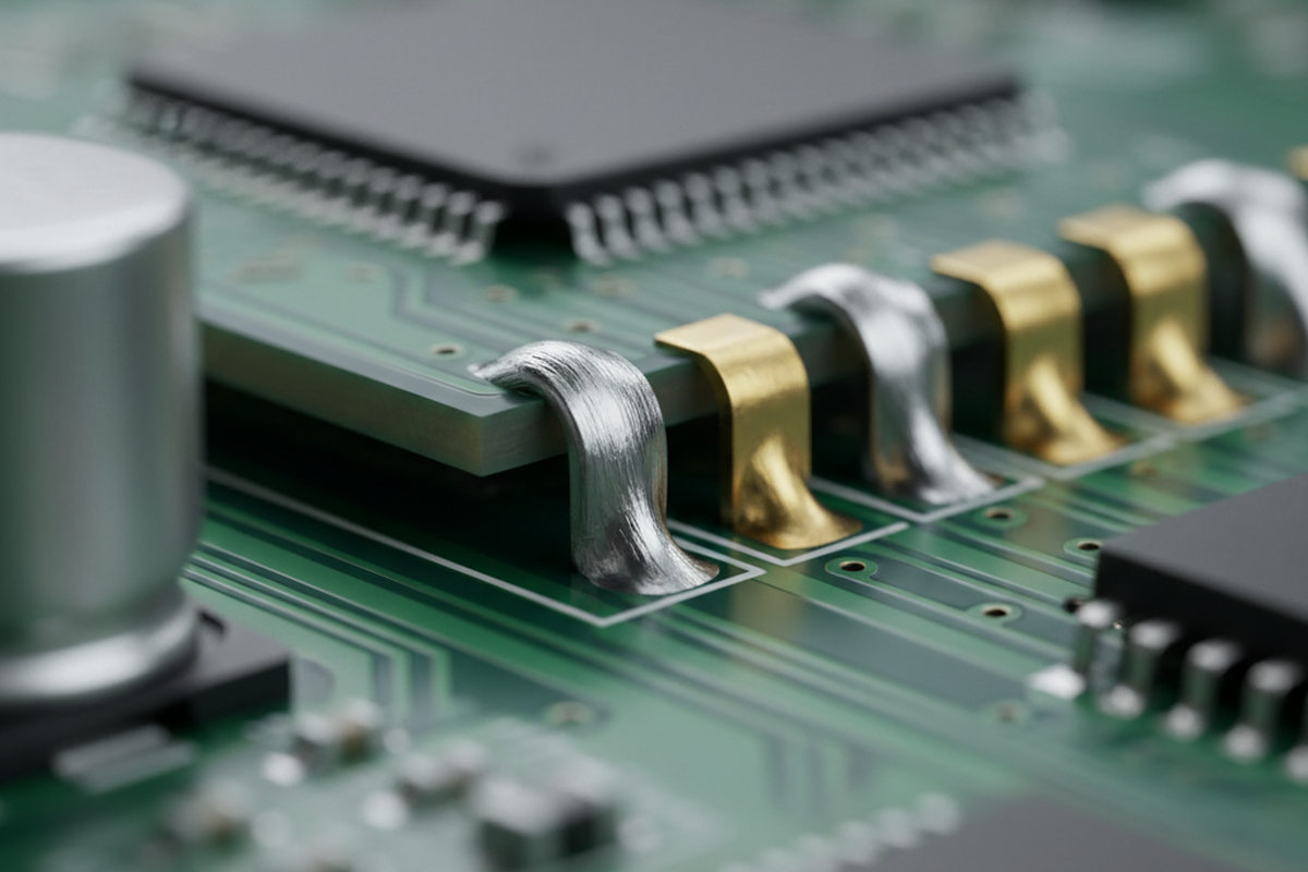
This is why “sufficient” solder isn’t enough. The joint needs a specific shape—a robust fillet—to distribute these forces. A flat, starved joint created by a 1:1 footprint copy might pass a basic electrical continuity test at the factory, but it has zero fatigue life. It is a ticking clock.
The Datasheet Footprint is Usually Wrong
The single most common cause of castellated joint failure is blindly following the “Recommended Land Pattern” in the module vendor’s datasheet. This sounds counterintuitive—surely the manufacturer knows best? But vendor incentives rarely align with your reliability requirements. They want to market the module as “compact” and “space-saving.” So their recommended footprints often shrink the pads to the absolute minimum, allowing you to route traces tightly around the device.
For high-reliability applications, ignore these suggestions and design for the fillet. The critical dimension is the “Toe”—the portion of the pad that extends outward, away from the module edge. A standard vendor footprint might give you 0.1mm or 0.2mm of toe projection, which is barely enough to form a meniscus. For a Class 2 or Class 3 assembly per IPC standards, you need a visible, inspectable solder fillet that climbs the wall of the castellation.
The rule of thumb for robust design is to extend the mainboard pad at least 0.5mm to 0.8mm beyond the edge of the module. This extra copper acts as a reservoir and a runway. During reflow, it holds a larger volume of solder paste; as the flux activates, surface tension pulls that extra solder up the vertical wall of the castellation. This creates a concave, stress-distributing slope rather than a brittle butt-joint.
If you are designing your own footprints, ensure you are looking at the correct view. It is distressingly common to see Version 1 boards where the footprint is mirrored because the designer looked at the “bottom view” of the module and applied it to the “top view” of the board. You are looking through the board, not at it. Double-check pin 1.
You Are Designing the Stencil, Not Just the Board
Geometry is only half the battle; volume is the other. A castellated joint requires significantly more solder paste than a standard flat pad because the solder has to defy gravity. It must wet the pad and then climb vertically up the half-cut hole. If you use a standard stencil aperture that matches the copper pad 1:1, you will likely end up with “insufficient wetting” rejects. The volume of paste printed on the flat pad simply isn’t enough to coat the vertical wall once the volatiles in the flux burn off.
You have to force the process by overprinting the aperture. The stencil opening for a castellated pad should be larger than the copper pad itself, specifically extending further outward. A common modification is to increase the aperture length by 10% to 20% in the direction away from the module. When the solder melts, it will pull back onto the gold or tin plating of the pad (since solder won’t stick to the solder mask), creating a “hump” of molten metal that feeds the vertical wicking action.
Have this conversation with your assembly house. If they run a standard 4-mil or 5-mil foil without modification, your yield will suffer. You might see wetting, but X-ray inspection will reveal voids or thin connections that won’t survive a drop test.
Invisible Killers: Placement and Depanelization

Even a perfectly soldered module can be destroyed before it leaves the factory floor. The physical placement of the module relative to the board’s edge and break-tabs is a reliability variable that often gets overlooked until it’s too late.
Look at the “mouse bites”—the perforated tabs used to hold the PCB in the panel during assembly. When these tabs are snapped or routed out (depanelization), a shockwave of mechanical stress travels through the FR4. If a rigid castellated module sits too close to these stress points—say, within 5mm—that energy transfers directly into the nearest solder joints. Since the module is stiff and the board is bending, the solder joint fractures.
This damage is insidious because it is often invisible to the naked eye. The board might pass the functional test because the two fractured surfaces are still touching. But the first time the device vibrates in a truck or a pocket, the connection opens. Keep castellated modules away from the edges of the board, and strictly enforce a keep-out zone around depanelization tabs. If the design forces the module near the edge, insist on a router-cut depanelization process rather than a mechanical “pizza cutter” or manual snapping, which impart significantly higher torque.
A Note on Hand Soldering
There is a persistent demand, particularly in prototyping phases, to hand-solder these modules. While it is technically possible to make an electrical connection with a soldering iron, it is nearly impossible to create a reliable one.
The physics of heat transfer works against you. A soldering iron applies heat to a single point on the toe of the pad, struggling to heat the entire castellation barrel evenly. The result is often a “cold” joint at the top of the hole or a blob of solder that sits on the surface without truly intermetallic wetting. Without the uniform surface tension of a reflow oven, it is also difficult to control the volume, leading to bridged pins or starved joints. If you are forced to rework a module or prototype by hand, use hot air and a generous amount of flux to mimic the reflow environment as closely as possible, but understand that these joints should not be trusted for vibration testing.
Reliability is a Choice
The failure of a castellated module is rarely a mystery. It is a predictable outcome of physics acting on insufficient metal. By extending the toe of the footprint, overprinting the stencil, and respecting the mechanical stress of the board, you convert a fragile connection into a robust structural element. It costs nothing in terms of BOM, but it requires the confidence to overrule the datasheet and design for the reality of the manufacturing floor.


 Circuit Board Assembly")


