The design is perfect. Robust components, an optimized thermal layout, flawless simulations. Then, weeks or months after launch, the field reports trickle in. The power stage is overheating. Performance is throttling. In the worst cases, components are failing outright. The culprit isn’t a flaw in your design. It’s a void: a microscopic bubble of gas trapped in the solder joint.
These voids are the silent killers of power electronics. For components like DPAKs, D2PAKs, and large QFNs mounted over heavy copper pours, a void is more than a cosmetic blemish; it is a direct threat to the reliability and lifetime of your product. At Bester PCBA, we don’t leave thermal performance to chance. We have engineered a systematic approach to hunt down and eliminate these voids where they are most dangerous.
Why Your Power Stage Is a Ticking Thermal Time Bomb
A solder void is a pocket of air. Air is an excellent thermal insulator. When a void forms under the primary thermal pad of a power component, it chokes the intended pathway for heat to escape into the circuit board. Instead of a wide, uniform connection to the copper heat sink, heat is forced to navigate around these insulating pockets. This constriction creates localized hot spots, causing the component’s junction temperature to spike far beyond what your datasheets and simulations predicted.
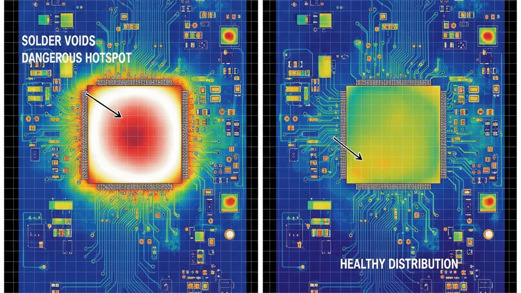
The consequences are not theoretical. A significant void percentage can easily raise the junction temperature by 20°C or more under load, drastically shortening the component’s operational life and compromising the reliability of the entire system.
The Physics of Voids: How Solder Paste Becomes a Heat Trap
Voids are born from the solder paste itself. The paste is a mixture of metal solder spheres and a viscous flux. During reflow, the flux becomes highly active, cleaning the metal surfaces to ensure a good bond. A byproduct of this activation is outgassing, where the flux releases volatile compounds as it heats. In a standard reflow process, these gas bubbles must escape from the molten solder before it solidifies.
When soldering a small component to a small pad, the outgassing has a very short and easy escape path. The problem becomes critical when dealing with large thermal pads.
DPAKs and Large Copper Pours: The Perfect Storm for Failure
A D2PAK sitting on a massive copper pour creates the ideal environment for trapping these gas bubbles. The large surface area of the thermal pad means a significant volume of flux is outgassing simultaneously. The distance from the center of the pad to the edge is long, giving a gas bubble a difficult journey to freedom. As the solder begins to solidify from the outside in, escape routes are sealed off, trapping the voids permanently. The result is a solder joint that looks solid on the outside but is internally compromised, like a structural beam riddled with air pockets.
The Flaw in “Good Enough”: Why Standard Reflow Fails
A standard convection reflow oven is fundamentally incapable of solving this problem. It applies heat, but it offers no mechanism to help the trapped volatiles escape. The process relies on the hope that bubbles will find their way out before the solder solidifies—a hope frequently dashed on power-dense designs.
Some operations turn to a basic vacuum reflow oven, thinking reduced pressure is a magic bullet. But applying a sudden, deep vacuum to molten solder is a blunt-force approach. It can cause the solder to bubble violently, leading to spatter that creates shorts or solder balls that compromise assembly cleanliness. Without precise control, a basic vacuum creates more problems than it solves. It is not a substitute for a disciplined process.
The Bester PCBA Playbook: A System for Void-Free Assembly
At Bester PCBA, we treat void reduction not as a single step, but as an integrated system. Our process combines stencil engineering, advanced vacuum profiling, and strict process discipline to ensure the highest integrity solder joints for void-sensitive components.
It Starts with the Stencil: Engineering Solder Paste Deposits

Before the board ever enters the oven, we engineer the solder paste deposit to fight voids. Instead of a single, large aperture for a thermal pad, we often specify a “windowpane” pattern. This design breaks the large deposit into smaller pads with defined channels between them. These channels act as dedicated outgassing pathways, giving flux volatiles a clear route to escape from under the component during the initial phases of reflow. A simple but profoundly effective first line of defense.
The Art of the Vacuum Profile: Controlled Pressure Ramps
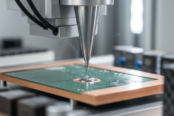
Once the solder is molten, our vacuum reflow ovens don’t just apply a crude vacuum. We execute a carefully programmed pressure profile. We reduce the pressure in controlled, gentle ramps, allowing smaller voids to coalesce and expand slowly. This gentle coaxing draws the trapped gas out of the solder without causing the violent boiling that leads to spatter. By precisely managing pressure, temperature, and timing, we evacuate the voids while maintaining the stability and form of the molten solder joint.
The Unsung Hero: Preheat Discipline and Flux Activation
Even the most advanced vacuum profile is useless without disciplined preheat and soak stages. Our process places immense emphasis on this. We ensure the entire assembly is brought to a uniform temperature, allowing the flux to perform its cleaning action and begin outgassing in a controlled manner before the solder reaches its liquidus temperature. This ensures that by the time the vacuum is applied, the flux has done its job and the bulk of the volatiles have already been released, leaving the vacuum to handle only the most stubborn, trapped bubbles.
Beyond Wishful Thinking: Verifying Thermal Integrity
We don’t operate on wishful thinking; we operate on proof. Our process is built on a foundation of verification, using industrial inspection tools to confirm the results of our work.
X-Ray Inspection: Seeing the Voids We Eliminated
After assembly, we use 2D and 3D X-ray inspection systems to look directly through components and into the solder joints. This allows us to quantify the voiding percentage with high precision. While industry standards might accept voiding as high as 25%, our vacuum reflow process routinely achieves percentages in the low single digits for critical thermal pads. This data provides objective, quantitative proof of a structurally sound connection.
Infrared Thermography: Proving the Thermal Performance

A low void percentage is only half the story. The ultimate goal is superior thermal performance. To close the loop, we verify this directly. By powering up the assembled board and viewing it with a high-resolution infrared camera, we analyze the thermal gradients across the power stage in real time. This IR analysis confirms that our low-void solder joints are effectively transferring heat away from the component, keeping junction temperatures low and ensuring the product will perform reliably in the field. We replace assumptions with thermal data.
The Real Cost of a Solder Void
An advanced process like vacuum reflow represents a greater upfront investment than a standard convection run. We encourage our clients to consider the alternative. What is the cost of a product recall? The engineering cost of a board redesign to compensate for a manufacturing defect? The damage to your brand’s reputation when a flagship product fails?
A solder void is a hidden liability baked into your hardware. The cost of that single bubble of trapped gas can echo through your entire business, manifesting in warranty claims, lost sales, and eroded customer trust.
At Bester PCBA, our vacuum reflow process isn’t just a service; it’s insurance against these hidden liabilities. It is an investment in product reliability, user safety, and brand integrity. We provide the manufacturing expertise that ensures your brilliant design performs exactly as you intended.
