There is a specific type of silence that falls over a fabrication floor when a new data package arrives with perfect, ninety-degree square openings in the coverlay layer. It is the silence of a CAM engineer anticipating the inevitable Engineering Query (EQ)—or worse, the silence of a scrap bin filling up three weeks later.
To the designer sitting in front of a high-resolution monitor, those sharp corners look crisp, professional, and precise. They match the orthogonal logic of the rigid boards they have spent a career routing. But in the physical world of flexible circuits, where materials are subjected to heat, pressure, and repeated mechanical bending, those sharp corners are structural liabilities.
Physics does not care about the aesthetic preferences of your CAD layout. When a flexible circuit bends, forces distribute across the surface until they hit a discontinuity. A square corner in the coverlay—the polyimide insulation layer laminated over the copper—acts as a massive stress riser. It focuses the mechanical energy of the bend into a single microscopic point on the underlying copper trace. The result is a board that passes every Design Rule Check (DRC) in the software but fails catastrophically the first time it is installed in a hinge or a tight enclosure.
The Geometry of the Murder Weapon
You cannot treat coverlay openings like rigid soldermask. You have to visualize the stack-up not as a single board, but as a sandwich of disparate materials fighting each other. The base is polyimide; the conductor is copper; the top layer is coverlay. When this sandwich bends, the outer layers stretch and the inner layers compress.
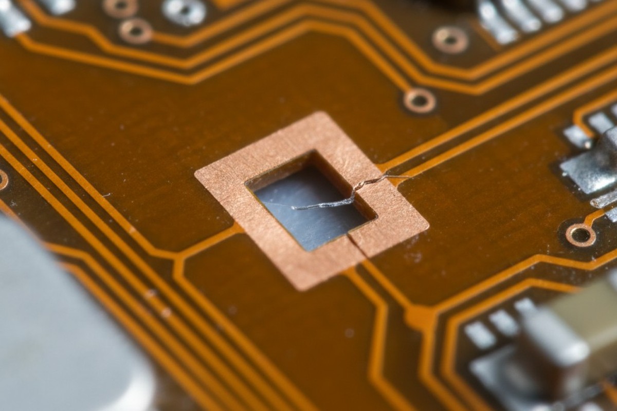
If the coverlay has a sharp, ninety-degree corner crossing over a copper trace, it creates a “mechanical notch.” The coverlay is stiffer than the adhesive beneath it, so it acts like a knife edge pressing into the copper every time the flex is manipulated.
Designers often point to modern laser cutting as a defense. They argue that lasers can ablate the polyimide in a perfect square without the radius limitations of a mechanical CNC drill bit. This is technically true but practically irrelevant. The capability of the tool does not negate the mechanics of the material. Even if the shop cuts a perfect square, the stress concentration remains. The copper trace running underneath that corner will experience a spike in strain that can be 3 to 5 times higher than in the surrounding areas.

In dynamic applications—like a sliding sensor in a camera or a laptop hinge—this is where the crack initiates. It propagates from the edge of the coverlay opening, through the copper, and leads to an open circuit after fewer than 1,000 cycles.
The fix is trivial in design but critical in function: every coverlay opening must have a radiused corner. Standard practice dictates a minimum corner radius of 0.2mm (roughly 8 mils). This allows the stress to distribute over a curve rather than focusing on a point. If the design allows, a larger radius is always better.
For those attempting to route traces near these openings, the “tear-drop” or fillet rule applies. The transition from the covered area to the exposed pad should never be abrupt. A simple 0.2mm fillet solves the entire structural issue, turning a potential field failure into a robust interconnect.
The Ooze Factor: Adhesive is a Liquid
The second fundamental issue is the nature of the attachment itself. Unlike the liquid photoimageable soldermask (LPI) used on rigid boards, which cures into a hard shell, coverlay is a solid sheet of polyimide glued down with an acrylic or epoxy adhesive.
During the lamination process, the stack-up is subjected to high heat and pressure. At this stage, the adhesive liquefies. It moves. It flows.
This “squeeze-out” is the enemy of high-density interconnects. If a designer creates a coverlay opening that matches the copper pad size exactly (1:1), the adhesive will inevitably ooze out onto the pad surface during lamination. This ooze is often transparent and microscopic, forming an invisible barrier between the gold or tin finish and the component lead.

The assembly house will report this as a “pad wetting failure” or “defective plating.” They will send photos of solder balling up and refusing to adhere to the pad. The root cause, however, isn’t the plating chemistry. It’s the physics of lamination. The adhesive flowed 0.05mm to 0.15mm onto the pad, insulating it.
Because adhesive flow varies based on the age of the pre-preg, the pressure of the lamination press, and the specific material brand (DuPont Pyralux vs. generic equivalents), the design must account for the worst-case scenario. The industry standard is to oversize the coverlay opening by at least 0.25mm (10 mils) larger than the pad it exposes. This provides a “dam” area where the adhesive can flow without encroaching on the solderable surface.
For extremely tight pitches where 10 mils of space does not exist, the designer must specify “low-flow” adhesives or switch to Laser Direct Imaging (LDI) soldermask, though that comes with its own set of mechanical risks.
Anchors and Material Myths
In the rigid world, copper adhesion to the FR4 core is incredibly strong. In the flex world, copper is effectively floating on a layer of soft polymer. When heat is applied during reflow or hand soldering, the thermal expansion mismatch can cause small copper pads to peel right off the base material. This is “pad lifting,” and it is a leading cause of rework scrap.
Coverlay helps hold pads down, but only if the opening is designed to trap the copper. A simple rectangular pad fully exposed by a larger coverlay opening has no mechanical retention. It is relying entirely on the chemical bond of the adhesive.
To fix this, designers must use “anchors,” “spurs,” or “bunny ears”—protrusions of copper that extend underneath the coverlay. The coverlay acts as a mechanical clamp, holding the spur down so the main pad cannot lift during soldering.

There is often a temptation to bypass all these geometric headaches by simply using Liquid Photoimageable (LPI) soldermask—the green stuff—on flex circuits. It allows for tighter dams and square corners. However, LPI is brittle. In a static application (install-to-fit), it is acceptable. But in any dynamic application, LPI will crack like dried mud on a bending riverbank. Once the mask cracks, it propagates into the copper, cutting traces just as effectively as a square coverlay corner. Unless the application is strictly static, standard polyimide coverlay is mandatory.
The Fabrication Floor Rules
To keep a design out of the engineering query queue and ensure high yield on the fabrication floor, a few non-negotiable rules apply. These aren’t aesthetic suggestions. They are requirements for mechanical survival.
- Radiused Corners: All coverlay openings must have a minimum corner radius of 0.2mm. No sharp squares.
- Oversize for Squeeze-Out: Openings should be 0.25mm (10 mils) larger than the pad to account for adhesive flow.
- Anchors for Pads: Any unsupported pad needs copper spurs extending at least 0.15mm under the coverlay to prevent lifting.
- Teardrops: All trace-to-pad transitions must be teardropped to prevent cracking at the junction.
Reliability in flexible circuits is defined by the weakest corner. By respecting the material properties of the coverlay and the adhesive, the design moves from a theoretical model in CAD to a functioning reality in the field.


 PCB Technology: Types, Benefits, Challenges, and Applications")


 Circuit Board Assembly")