In this article, we will delve into the world of PCBs and PCBA, exploring their definitions, materials, applications, and manufacturing processes. Whether you’re a tech enthusiast or simply looking to expand your knowledge, this comprehensive guide will provide you with a clear understanding of the difference between PCB and PCBA. So, let’s dive in and unravel the mysteries of these essential components in the world of electronics.
What Is the PCB
A printed circuit board (PCB) is an electronic component that serves as a support and carrier for electronic components, facilitating electrical connections between them. It is often referred to as a “printed” circuit board because it is created through a process of electronic printing. PCBs are made from non-conductive materials, such as fiberglass or composite epoxy, with a layer of conductive material, typically copper, on one or both sides.
The primary function of a PCB is to provide a reliable and efficient means of connecting and supporting electronic components. By offering a standardized platform for component placement and interconnection, PCBs eliminate the need for complex wiring and soldering. This simplifies the assembly process and enhances the overall reliability and performance of electronic devices. PCBs are also marked with silkscreen to show the position and names for the components.
PCBs come in various sizes and shapes, catering to the specific requirements of different applications. They can range from small, single-layer boards used in simple devices like calculators to complex, multi-layer boards employed in advanced electronics such as smartphones and computers.
The conductive pathways on a PCB, known as the circuit layout, are designed to establish electrical connections between the components. These pathways are created by etching the conductive material into a specific pattern. The circuit layout determines how the components communicate and work together to perform specific functions.
PCBs find applications in a wide range of industries and sectors, including consumer electronics, industrial machinery, robotics, vehicles, and medical equipment. They provide a stable and reliable platform for the integration of electronic components, ensuring the proper functioning of electronic devices.
Materials Used in PCBs
PCBs are composed of various materials that are responsible for their performance and functionality. Let’s take a closer look at the materials used in PCB fabrication.
Substrate
The substrate material serves as the base of the PCB and provides mechanical support. It is typically made of a non-conductive material, such as fiberglass-reinforced epoxy resin (FR-4). FR-4 is widely used due to its excellent electrical insulation properties, high mechanical strength, and cost-effectiveness.
Copper Foil
Copper foil is laminated onto the substrate material to create conductive pathways. It serves as the conductive layer for the PCB. Copper is chosen for its high electrical conductivity and corrosion resistance. The thickness of the copper foil can vary depending on the application and design requirements.
Prepreg
Prepreg, which is a glass fabric coated with resin, such as FR4 epoxy resin, polyimide, or Teflon, acts as an insulating layer between the copper layers in multi-layer PCBs. Laminates, also known as copper-clad laminates, are composed of sheets of prepreg laminated together with heat and pressure. They form the core structure of the PCB, providing rigidity and stability.
Solder Mask
The solder mask is a protective layer applied over the copper traces to prevent short circuits and oxidation. It is usually green in color, but other colors like red, blue, or black can also be used. The solder mask provides insulation and protects the copper traces from environmental factors, such as moisture and dust.
Silkscreen
The silkscreen layer is used to add component labels, reference designators, and other markings on the PCB. It is usually white in color and helps in identifying components and their placement during assembly and troubleshooting.
Flexible Materials
In addition to these materials, flexible PCBs are another type of PCB that is constructed with flexible materials. These flexible PCBs can be single-layer, double-layer, or multi-layer and are designed to withstand repeated flexing. They are commonly found in modern devices like laptops, cell phones, and robotic arms.
PCB manufacturers can create reliable and efficient circuit boards for a wide range of applications by carefully selecting and utilizing these materials. The materials used in PCB fabrication are essential for ensuring the functionality, durability, and reliability of the PCBs. Each material serves a specific purpose, from providing mechanical support to creating conductive pathways and protecting against environmental factors.
The selection of materials depends on factors such as dielectric constant, flame retardance, loss factors for high-speed applications, mechanical strength, and thermal performance. PCB manufacturers consider these factors to ensure that the materials used meet the specific requirements of the PCB design and the intended application.
Applications of a PCB
PCBs, or printed circuit boards, have a wide range of applications across various industries. They are an essential component in many electronic devices that we use in our daily lives. Let’s explore some of the common applications of PCBs:
Consumer Electronics
PCBs are extensively used in consumer electronics such as smartphones, tablets, laptops, televisions, and gaming consoles. They provide the necessary circuitry for these devices to function efficiently and compactly.
Automotive Industry
PCBs are widely used in the automotive industry, where they are used in engine control units (ECUs), dashboard electronics, entertainment systems, and safety systems. PCBs used in automobiles need to be durable and reliable to withstand the harsh environmental conditions.
Medical Devices
PCBs are widely used in medical devices and equipment, including pacemakers, defibrillators, ultrasound machines, and medical imaging systems. These devices require high precision and accuracy, and PCBs ensure the proper functioning of these critical medical devices.
Industrial Equipment
PCBs are used in industrial equipment for automation, control systems, and monitoring. They are found in machinery used in manufacturing, power generation, robotics, and process control. PCBs used in industrial applications need to be rugged and able to withstand challenging conditions.
Aerospace and Defense
PCBs are critical components in aerospace and defense systems, including avionics, communication systems, radar systems, navigation systems, and missile guidance systems. PCBs used in these applications need to meet stringent quality and reliability standards.
Telecommunications
PCBs are used in telecommunications equipment such as routers, switches, modems, and base stations. These devices require high-speed and high-frequency circuitry, and PCBs enable efficient signal transmission and processing.
Renewable Energy
PCBs are used in renewable energy systems such as solar panels and wind turbines. They help in controlling and monitoring the power generation process, ensuring efficient and reliable operation.
IoT Devices
With the rise of the Internet of Things (IoT), PCBs have become essential in connecting and controlling various smart devices. They are used in smart home systems, wearable devices, home automation, and other IoT applications.
In addition, PCBs are also used in lighting equipment, maritime industry, calculators, data storage equipment, and more. The versatility, reliability, and ability of PCBs to handle high-density wiring make them an integral part of modern electronic devices across various industries.
The applications mentioned here are not an exhaustive list, but rather a representation of the wide range of industries and devices where PCBs are used. The continuous advancements in technology and the increasing demand for electronic devices ensure that the applications of PCBs will continue to expand in the future.
Different Types of PCB
There are several different types of PCBs, each with its own unique characteristics and applications. By understanding the different types of PCBs, you can make an informed decision when selecting the right PCB for your project. Whether you need a simple single-layer PCB or a complex multi-layer PCB, each type has its own advantages and is suitable for different applications. Consider factors such as the complexity of the circuit, the space available, the required flexibility, and the durability needed for your specific electronic device. Let’s take a closer look at these types to provide a more comprehensive understanding.
Single-Layer PCB
A single-layer PCB, also known as a single-sided PCB, is the simplest type of printed circuit board. It consists of a single layer of conducting material, typically copper, on one side of an insulating substrate. The conductive layer is etched to create the desired circuit pattern, connecting the various components and traces on the board.
Single-layer PCBs are commonly used in electronic devices with simpler circuitry and fewer components. They are cost-effective and relatively easy to manufacture compared to other types of PCBs. One advantage of single-layer PCBs is their ease of design and production. They are commonly used in low-cost, high-volume applications such as printers, radios, and calculators. The single layer of conducting material is typically coated with a layer of solder mask to protect it from oxidation. Components are marked on the PCB using a silkscreen.
Single-layer PCBs may not be suitable for devices that require a higher number of components and connections. The single layer limits the available space for traces and components, which can be a constraint when designing circuits with higher density or complex routing. Careful planning and optimization of component placement and trace routing are necessary to maximize the available space.
Double-Layer PCB
A double-layer PCB, also known as a two-layer PCB, is a type of printed circuit board that consists of two layers of conductive material separated by an insulating layer. This type of PCB is commonly used in a wide range of electronic devices and applications.
The construction of a double-layer PCB involves the use of a substrate material, typically fiberglass or epoxy, which provides mechanical support and insulation. On top of the substrate, a layer of copper is applied, serving as the conductive material for the circuit. The copper layer is etched to create the desired circuit pattern, leaving behind the traces and pads that will be used to connect the electronic components.
Double-layer PCBs can accommodate more complex circuit designs compared to single-layer PCBs. With two layers of conductive material, it is possible to create more intricate and dense circuitry, allowing for increased functionality and performance. This makes double-layer PCBs suitable for applications that require higher levels of complexity, such as consumer electronics, automotive systems, and industrial control systems. Double-layer PCBs offer improved signal integrity and reduced electromagnetic interference (EMI) compared to single-layer PCBs. The presence of a ground plane on the second layer helps minimize noise and interference, resulting in better overall performance and reliability of the electronic device.
Multi-Layer PCBs
Multi-layer PCBs, as the name suggests, are printed circuit boards that consist of more than two conductive layers of copper. These boards are designed to accommodate complex applications that require a higher number of components and connections. The multiple layers of conductive material provide increased circuit density, making multi-layer PCBs more powerful, durable, and compact compared to single-layer or double-layer PCBs.
Multi-layer PCBs can handle intricate circuitry in a smaller footprint. By utilizing multiple layers, designers can create complex electronic systems that would be impossible to achieve with single-layer or double-layer PCBs. This makes multi-layer PCBs ideal for applications such as satellite systems, GPS technology, file servers, data storage equipment, and medical devices.
The construction of a multi-layer PCB involves sandwiching layers of conductive material between insulating layers, with glue securing the layers together. This ensures that the circuit is not damaged by excess heat and provides stability to the board. The multiple layers are interconnected through vias, which are small holes drilled through the insulating layers and plated with conductive material. These vias allow electrical signals to pass between different layers of the PCB, enabling the circuit to function as intended.
Flexible PCBs
Flexible PCBs, also known as flex circuits or flex boards, are a type of printed circuit board that offers flexibility and bendability. They are made up of printed circuits and components arranged on a flexible substrate, which is commonly made from materials such as polyamide, PEEK, or a transparent conductive polyester film. Flexible PCBs can be designed in single-sided, double-sided, or multilayer configurations.
Flexible PCBs are famous for their ability to save space. Due to their flexibility, they can be bent or folded to fit into tight spaces, allowing for more compact designs. This makes them ideal for applications where space is limited, such as in portable electronics like smartphones and laptops.
Another advantage is the elimination of connectors. By integrating the flexible PCB directly into the device, the need for connectors is reduced, resulting in a more streamlined and compact design. This not only saves space but also simplifies the assembly process and can contribute to cost savings.
Flexible PCBs also offer improved thermal management. The flexibility of the substrate allows for better heat dissipation, which helps prevent overheating and improves the overall performance and reliability of the device. This is particularly important in applications where heat generation is a concern, such as in high-power electronics or devices that operate in harsh environments.
Rigid PCBs
Rigid PCBs are the most common type of PCBs used in electronic devices. They are made from a solid, inflexible substrate material such as fiberglass-reinforced epoxy laminate. Rigid PCBs provide a sturdy and rigid platform for mounting electronic components and interconnecting them with copper traces. They come in different configurations, including single-sided, double-sided, and multi-layer designs.
Rigid PCBs are cost-effective. They are generally more affordable compared to other types of PCBs due to their simpler construction and manufacturing process. Additionally, rigid PCBs offer ease of diagnostics and repair. The rigid nature of these boards allows for easy access to components, making troubleshooting and component replacement more convenient.
They also provide better electrical performance and lower electronic noise compared to flexible PCBs. The solid substrate of rigid PCBs offers improved insulation, reducing the chances of signal interference. This makes them suitable for applications where signal integrity is crucial.
Another advantage is the mechanical stability. They can absorb vibrations, making them ideal for devices that may be subjected to vibrations or shocks. Additionally, rigid PCBs are compact and lightweight, making them suitable for applications where space is limited or weight reduction is desired.
Flex-Rigid PCBs
Flex-Rigid PCBs are a unique type of circuit board that combines elements from both flexible and rigid PCBs. These boards are designed to provide the benefits of flexibility and rigidity in a single board, making them ideal for applications that require both characteristics.
Flex-Rigid PCBs consist of multiple layers of flexible PCB material interconnected with layers of rigid PCB material. This combination allows the board to bend and flex in certain areas while remaining rigid in others. The flexible sections are typically made of materials like polyimide or polyester film, while the rigid sections are made of materials like FR4.
Flex-Rigid PCBs save space and reduce the need for connectors and cables. By integrating both flexible and rigid sections into a single board, the overall size and weight of the electronic device can be reduced. This is particularly beneficial in applications where space is limited, such as in portable devices or wearable technology.
They also offer improved reliability compared to using separate flexible and rigid boards. The elimination of connectors and cables reduces the risk of connection failures and improves signal integrity. Additionally, the use of flexible materials allows the board to withstand vibrations, shocks, and thermal expansion, making it more durable in harsh environments.
What Is the PCBA
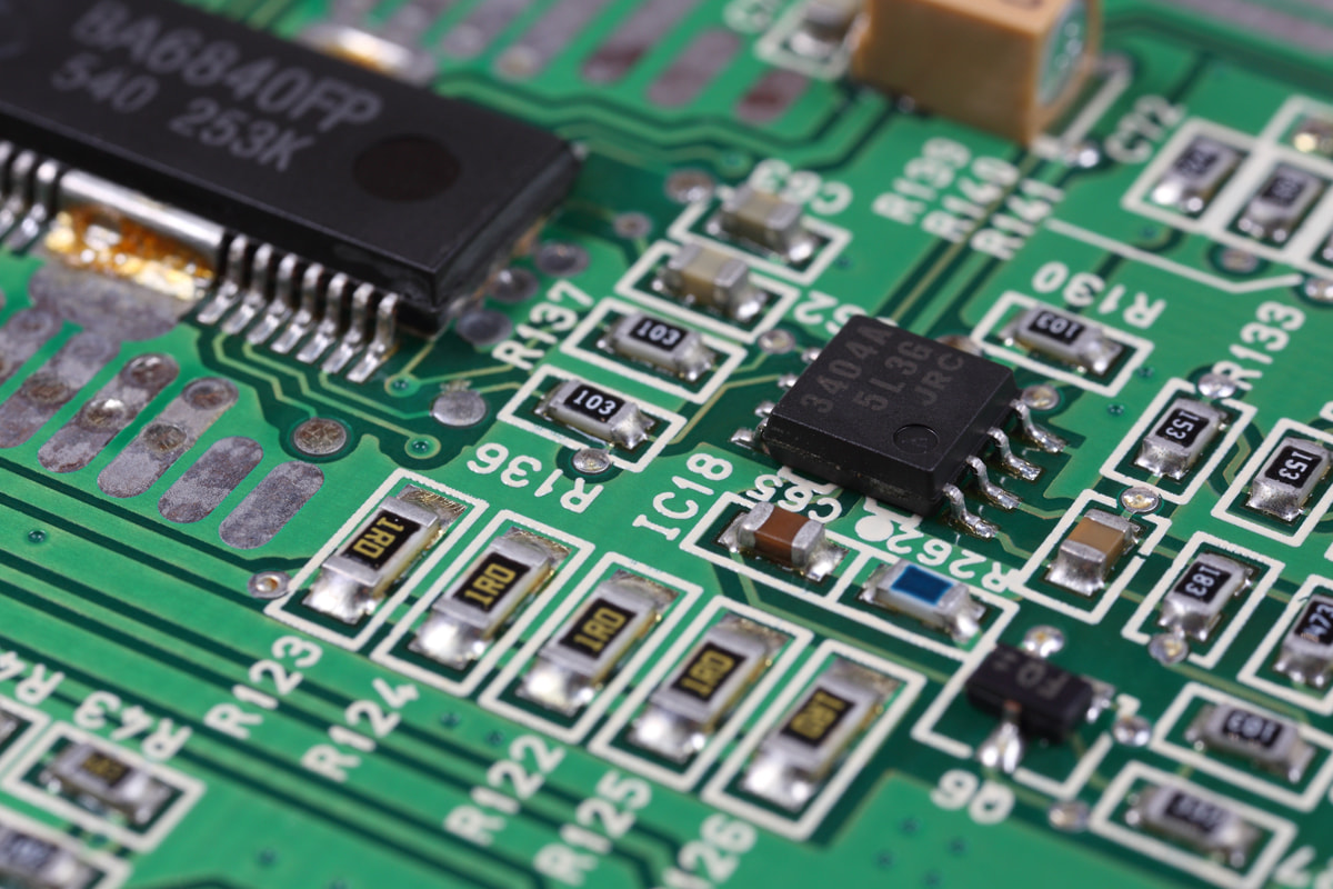
Printed circuit board assembly (PCBA) is the process of assembling electronic components onto a printed circuit board to create a fully functional circuit board. It involves the placement and soldering of components onto the designated pads and traces on the PCB.
The PCBA process includes several steps. First, the bare PCB is manufactured by creating a conductive pattern on an insulating substrate. This pattern serves as the foundation for the electrical connections between components. The PCB can be single-layer, double-layer, or multi-layer, depending on the complexity of the circuit design.
Once the PCB is ready, it goes through the surface-mount technology (SMT) process. In this process, surface-mount components, such as resistors, capacitors, integrated circuits, and connectors, are placed and soldered onto the PCB using automated machines. SMT allows for precise component placement and high-speed assembly, making it suitable for mass production. In addition to SMT, through-hole technology (THT) may be used for certain components that require a stronger mechanical connection or higher power handling capability. THT involves drilling holes in the PCB and inserting the leads of the components into these holes. The leads are then soldered on the opposite side of the board, either manually or using wave soldering machines.
Once all the components are attached, the PCBA undergoes testing, inspection, and quality control to ensure its functionality and reliability. Various testing methods, such as visual inspection, automated optical inspection, and functional testing, are employed to detect any defects or issues in the assembly. This ensures that the PCBA meets the required specifications and standards.
Applications of PCBAs
PCBA has a wide range of applications across various industries the same as PCBs. These assemblies are used in electronic devices and equipment to provide connectivity and functionality. Let’s explore some of the common applications of PCBA:
Consumer Electronics
PCBAs are extensively used in consumer electronics such as smartphones, tablets, laptops, televisions, and gaming consoles. They serve as the backbone of these devices, providing the necessary circuitry for power distribution, signal processing, and user interface. Additionally, PCBAs are used in kitchen appliances and entertainment systems.
Industrial Equipment
PCBAs are used in industrial equipment for automation, control, and monitoring purposes. They are used in machines, power converters, power measuring devices, and industrial control systems. PCBAs designed for industrial applications are built to withstand harsh conditions, including heat, moisture, and chemicals.
Automotive Industry
PCBAs are integral components in the automotive industry, where they are used in engine control units (ECUs), infotainment systems, dashboard displays, sensors, and lighting systems. These assemblies ensure reliable and efficient operation of various systems in vehicles.
Medical Devices
PCBAs are vital in the medical field, where they are used in medical imaging systems, patient monitors, diagnostic equipment, and surgical instruments. These assemblies enable accurate data processing, precise control, and reliable performance in medical devices. High-density interconnect HDI PCBs are specially designed for medical applications that require precision and high accuracy.
Telecommunications
PCBAs are extensively used in the telecommunications industry for devices such as routers, switches, modems, and base stations. They provide the necessary circuitry for data transmission, signal processing, and network connectivity.
Aerospace and Defense
PCBAs are critical in the aerospace and defense industry, where they are used in avionics systems, communication equipment, radar systems, navigation systems, and missile guidance systems. These assemblies are designed to withstand extreme conditions and ensure reliable performance in demanding environments.
Energy and Power Systems
PCBAs are used in energy and power systems for control, monitoring, and protection purposes. They are used in inverters, power converters, smart meters, and renewable energy systems. PCBAs in these systems ensure efficient power conversion and reliable operation.
Other Applications
PCBAs are also used in various other applications, including illumination and lighting systems, maritime industry equipment, data storage equipment, and video game systems.
Components of PCBA
During the assembly process of a PCBA, an empty PCB board is populated with electronic components to form a functioning printed circuit assembly. The components used in a PCBA can be categorized into passive and active electronic components.
Passive Components
Passive components, such as resistors and capacitors, control voltage levels, filter out noise and provide signal conditioning. Transformers are also used to transfer electrical energy between different circuits and adjust voltage levels. These components are for the proper functioning of the circuit.
Active Components
Active components, including integrated circuits (ICs), transistors, and diodes, are responsible for amplifying or switching electronic signals and power. ICs, which contain multiple devices on a single chip, perform various functions within the circuit. Transistors are used for amplification, oscillation, and digital logic circuits, while diodes allow current to flow in one direction and block it in the opposite direction.
Other Components
Connectors, relays, integrated passive devices (IPDs), and sensors are other components found in a PCBA. Connectors establish electrical connections between the PCBA and external devices or other PCBs. Relays act as electromechanical switches controlled by electrical signals. IPDs integrate passive components into a single chip, saving space on the PCB. Sensors detect and respond to physical or environmental changes, enabling various applications.
PCBA Process
The printed circuit board assembly process involves the assembly of electronic components onto a PCB to create a functional electronic device. There are different methods and technologies used in the PCBA process, including Surface-Mount Technology (SMT), Thru-hole technology, and Mixed Technology.
Note: before the PCBA process, careful sourcing of electronic components based on the design requirements of the PCB is required. Components like resistors, capacitors, integrated circuits, and microprocessor chips are selected during the design phase and then mounted onto the PCB using the appropriate assembly method.
Surface-Mount Technology (SMT)
Surface-Mount Technology (SMT) is a highly automated process used in the assembly of PCBs. It involves mounting electronic components directly onto the surface of the PCB, eliminating the need for drilling holes and inserting leads through the board.
The SMT process begins with the preparation of the PCB. Solder paste, which is a mixture of solder alloy and flux, is applied to specific areas where the components will be mounted. This solder paste acts as an adhesive and helps facilitate the soldering process.
- Next, the components are placed onto the solder paste using automated equipment such as pick-and-place machines. These machines accurately position the components onto the designated areas of the PCB. The sticky nature of the solder paste holds the components in place.
- Once the components are in position, the PCB is heated in a reflow oven. The oven raises the temperature of the PCB, causing the solder paste to melt and form a bond between the components and the PCB. This process is known as reflow soldering.
- During reflow soldering, the molten solder flows and creates a strong electrical and mechanical connection between the components and the PCB. The surface tension of the solder helps align the components properly, ensuring a reliable connection.
- After the reflow process, the PCB is cooled down, solidifying the solder and completing the SMT assembly. The resulting PCBA is compact, lightweight, and highly reliable due to the precise placement and soldering of the components.
SMT VS THT
SMT offers several advantages over traditional thru-hole technology. SMT allows for smaller and more densely packed PCB designs, as components can be placed on both sides of the board. This leads to more efficient use of space and enables the creation of smaller electronic devices.
SMT is also a faster and more automated process compared to THT. The use of pick-and-place machines and reflow ovens significantly speeds up the assembly process, reducing production time and costs.
In addition, SMT provides better electrical performance due to shorter signal paths and reduced parasitic capacitance and inductance. This results in improved signal integrity and higher-frequency operation.
Thru-Hole Technology (THT)
Thru-hole technology (through-hole technology or THT) is a method of assembling electronic components onto a PCB. This assembly process is used to mount thru-hole components on a PCB board. Thru-hole components have long leads that are inserted into pre-drilled holes on the PCB. These components are generally larger and cheaper compared to surface-mounted components.
The process of thru-hole technology begins with drilling holes into the PCB at specific locations. The leads of the components are then inserted into these holes and soldered to secure them in place. The solder not only holds the components firmly but also provides an electrical connection between the leads and the PCB.
THT is reliable and durable. The components mounted using this method are securely attached to the PCB, making them less susceptible to mechanical stress and vibration. This makes thru-hole technology suitable for applications that require high reliability, such as aerospace, automotive, and industrial electronics.
Thru-hole technology also allows for easy manual assembly and repair. Since the components are physically inserted into the pre-drilled holes, it is easier to visually inspect and replace faulty components if needed. This makes thru-hole technology a preferred choice for prototyping and low-volume production.
THT also offers better electrical connections in certain cases. The leads of the components are soldered on both sides of the PCB, providing a stronger and more stable connection. This is particularly important for components that handle high currents or require strong mechanical support.
However, the larger drill holes required for thru-hole components can limit the density of components that can be placed on the PCB, making it less suitable for compact and miniaturized electronic devices. Additionally, the manual assembly process of thru-hole technology is more time-consuming and labor-intensive compared to surface-mount technology (SMT), which can result in higher production costs for high-volume manufacturing.
Thru-hole technology is commonly used for components that require high mechanical strength, such as connectors, switches, and power devices. Thru-hole technology is also preferred for applications that involve high-power circuits, as it provides better heat dissipation compared to SMT.
Mixed Technology
Mixed technology, also referred to as hybrid technology, combines the advantages of both surface-mount technology (SMT) and thru-hole technology (THT) in the assembly process of a PCBA. This approach offers greater flexibility and efficiency in manufacturing, particularly in applications that require a combination of both assembly styles.
In mixed assembly, some components are mounted using SMT, while others are mounted using THT. This allows for a wider range of component options, as certain components may only be available in thru-hole packages or may be better suited for thru-hole mounting due to their size or electrical requirements. THT provides stronger mechanical connections, making it suitable for components that may experience higher levels of stress or require additional support. Additionally, it allows for the integration of legacy components that are only available in thru-hole packages. This is particularly useful when upgrading or repairing older electronic systems that still rely on these components.
The process of mixed technology assembly involves a combination of SMT and THT processes. SMT components are first mounted onto the PCB using automated pick-and-place machines and soldered onto the surface of the board using reflow soldering techniques.
After the SMT components are mounted, the PCB undergoes a secondary process to accommodate the thru-hole components. This involves drilling holes in the PCB where the thru-hole components will be inserted. The thru-hole components are then manually inserted into the drilled holes and soldered onto the PCB using wave soldering or hand soldering techniques.
Mixed technology offers the best of both worlds by combining the advantages of SMT and thru-hole technology. It allows for a wider range of component options, stronger mechanical connections, and the ability to integrate legacy components. This makes it a versatile and efficient option for PCBAs that require a combination of different component types. Mixed technology assembly also does not use solder paste, making it a necessary process for certain applications.
What Files Are Needed to Manufacture a PCBA
Several files are required to ensure accurate production and assembly of the PCBA process. These files provide the necessary information for the manufacturer to fabricate the PCB and assemble the components correctly. Let’s take a look at the essential files needed for PCBA manufacturing:
Gerber Files
Gerber files are open ASCII vector format files that show information on each board layer of a PCB design. They contain detailed information about the PCB layout, including the copper traces, pads, holes, and other design elements. Gerber files are generated by PCB design software and are typically provided in a compressed format (.zip or .rar) to ensure all necessary layers and data are included.
Bill of Materials (BOM)
The BOM is a comprehensive list of all the components necessary to put together the PCBA. It includes details such as part numbers, component descriptions, quantities, and reference designators. The BOM helps the manufacturer source the correct components and ensures that the assembly is accurate. It is important to optimize the BOM for mass manufacturing to streamline the production process.
Pick and Place File
This file shows all the components of the PCBA and their respective x-y coordinates and rotation. It is obtained from the PCB design software and is crucial for the automated assembly process. The pick and place file guides the pick-and-place machine to accurately place the components on the PCB, ensuring precise alignment and orientation.
In addition to these files, there are other files and documents that may be required depending on the specific requirements of the PCBA manufacturing process. These may include assembly drawings, test files (such as test point files, test fixture files, and test program files), and schematic diagrams. These additional files provide further instructions and specifications for the manufacturing and testing processes.
Customers should provide these files in the appropriate formats specified by the manufacturer. Common file formats include Gerber (RS-274X), Excel or CSV for BOM, and ASCII or CSV for pick and place files. Consulting with the manufacturer to confirm their specific file format requirements is recommended to ensure seamless communication and accurate production.
How to Analyze the Cost of PCBA
Analyzing the cost of PCBA involves considering several factors that can impact the overall price. Here are the key factors to consider:
Labor Costs
The cost of PCBA is influenced by the labor involved in the manufacturing process. Countries with lower wages tend to have cheaper labor costs, while countries with higher wages will have higher labor costs. It’s important to strike a balance between cost and quality when considering labor costs.
Tooling and Set Up Charges
If you require custom PCB shapes, you may need to pay for tooling and set up charges. However, if you opt for standard shape PCBs, you can avoid these additional costs. Analyze the design requirements and determine if custom shapes are necessary to minimize tooling and set up charges.
Turnaround Time
The speed at which you need your PCBA can affect the cost. Faster turnaround times typically come with higher costs, as manufacturers may need to prioritize your order, work extra hours, or pay for expedited shipping. Analyze your project timeline and budget to determine the optimal turnaround time.
Quantity
Economies of scale apply to PCBA manufacturing. Ordering larger quantities can lead to lower prices, especially for custom boards, as tooling and set up costs can be spread across multiple units. Conversely, ordering a small number of customized boards can result in higher costs. Analyze your production volume requirements and consider the impact on cost when making decisions.
Technology
The technology used in PCBA, such as Surface-Mount Technology (SMT) or Through Hole Technology, can impact the overall cost. SMT, being a highly automated process, can provide cost savings compared to Through Hole Technology. Analyze the requirements of your project and choose the appropriate technology that balances cost and functionality.
Packaging
The type of packaging required for your PCBs can also affect the cost. Ball grid array (BGA) packaging, which requires more time and effort to mount due to its many electrical pins, can result in higher assembly costs. Analyze the packaging requirements and consider the impact on cost when making decisions.
PCBA manufacturing in China is generally cheaper and faster compared to other countries. Chinese manufacturers often offer competitive prices and shorter turnaround times. Customers also need to evaluate other factors such as expertise, technology, and quality when considering alternatives in other countries.
How to Pick a PCBA Manufacturer
When selecting a PCBA manufacturer, the first thing to consider is the manufacturer’s capacity to handle your specific order. It’s essential to choose a manufacturer with the capability to fulfill a large quantity of boards if that is what you require. Additionally, inquire about the manufacturer’s overhead costs and manufacturing time, as these factors can impact the overall cost and timeline of your project.
Thorough testing of the PCBA design is another crucial consideration. It’s advisable to partner with a manufacturer whose engineers have already built a working prototype to avoid potential design issues in the future. Detecting electromagnetic issues ahead of time is also important to prevent any delays or problems down the road. Therefore, prioritize working with a PCBA manufacturer that emphasizes quality testing.
The number of layers on your board can also impact the cost and complexity of the manufacturing process. Boards with more layers may require additional time for building, testing, production, and assembly. Therefore, work with a PCBA manufacturer who takes into account factors such as size, weight, design, and function. Transparency about costs, technology, and design is crucial, and the manufacturer should be willing to collaborate with you to meet your specific needs.
Lead time is another key consideration. Ensure that the manufacturer guarantees timely delivery of the assembled boards, as delays could disrupt your production schedules or product launches. The manufacturer should provide a detailed Design for Manufacturability (DFM) report, which offers recommendations to enhance the manufacturability of your design and avoid potential manufacturing issues and costs.
Pricing is also a significant factor in the selection process. The costs quoted by the PCBA manufacturer should be competitive and subject to negotiation. A flexible pricing structure allows you to maximize the value of your investment. Discussing and bargaining with the manufacturer can help you manage your budget while ensuring you receive a high-quality product.
PCBA Cost in China vs. PCBA Cost in Asia
When it comes to the cost of PCBAs, China has traditionally been known for offering cheaper prices due to lower labor costs, but the cost is not solely determined by labor costs. Factors such as material costs, component availability, manufacturing capabilities, and quality control also determine the overall cost.
While China has been a dominant player in the PCB manufacturing industry, other low-wage Asian countries like Vietnam and India may offer lower operational costs. Still, when it comes to complex electronics manufacturing, these countries may lack the expertise and technology required.
One such country is Malaysia, which is emerging as an alternative for PCBA manufacturing. Even so, PCBA manufacturing in Malaysia tends to be more expensive and time-consuming compared to China. SMT efficiency in Malaysia is lower, and shipping component reels from China to Malaysia can be a hassle, especially for small runs. Labor costs in Malaysia can increase significantly each year, making it difficult to calculate costs accurately. Assembly workers in Malaysia tend to be slower compared to those in Shenzhen, China. As a result, PCBA manufacturing in Malaysia can be more expensive and time-consuming than in China.
Vietnam and India are also options to consider, as they offer lower operational costs, but they may lack the expertise and technology required for complex electronics manufacturing. Consider the specific requirements of your project and assess whether the chosen country can meet those needs effectively.
The cost of PCBAs is influenced by various factors, including labor costs, tooling charges, setup charges, turnaround time, quantity, technology, and shipping and packaging. Labor costs can vary between countries, with some countries offering cheaper labor but potentially lower quality expectations. Custom shapes and builds may incur additional setup charges, while standard PCB designs can help avoid these costs.
Turnaround time and quantity can also impact the cost of PCBAs. Expedited shipping and extra work time will generally increase costs, and the price of materials can fluctuate based on economic factors. The required technology, such as SMT or thru-hole tech, can also affect costs. SMT, for example, is a more automated process that can save money.
While PCBAs may generally be cheaper in China, customers should take the total cost, including shipping and logistics into consideration. The quality and expertise of the manufacturer should not be overlooked. Thoroughly researching and vetting potential manufacturers is crucial to ensure they meet quality standards. Choosing a manufacturer solely based on cost can lead to issues in the long run.
What Is the Difference Between PCB and PCBA
In simple terms, a PCB (Printed Circuit Board) is a bare circuit board with no electronic components and a PCBA (Printed Circuit Board Assembly) is the process of assembling electronic components to the PCB board. A bare PCB board without components cannot function, thus a PCBA can be seen as the complete circuit board as the finished product.
Here are the definitions of PCB and PCBA for your reference:
- A PCB, or Printed Circuit Board, is a flat board made of non-conductive material that serves as a base for electronic components. It provides mechanical support and electrical connections between various components on the board. PCBs can be made from different materials such as metal, ceramic, or FR4 (glass-reinforced epoxy laminate material). The choice of material depends on factors like durability, resistance to high temperatures, and cost. PCBs can also vary in flexibility and the number of layers they possess. They can be single-layered or dual-layered, depending on the complexity of the electronic device being designed.
- PCBA, or Printed Circuit Board Assembly, refers to the process of assembling electronic components onto a PCB. It involves soldering or attaching components like resistors, capacitors, integrated circuits, and connectors onto the PCB to create a functional electronic device. PCBA is typically done by specialized manufacturers who have the expertise and equipment to handle the assembly process.
 PCB Technology: Types, Benefits, Challenges, and Applications")

 Circuit Board Assembly")


