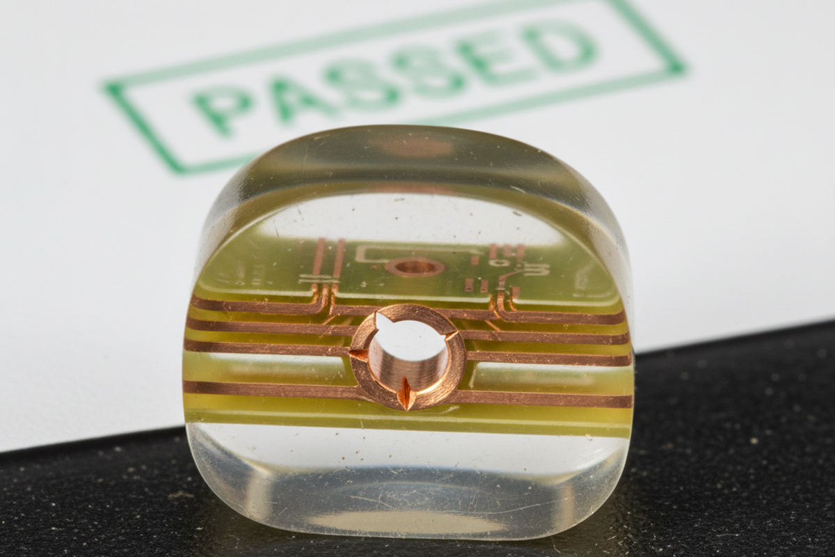
The board is dead. It was a high-stakes unit—perhaps an autonomous logistics controller or a medical monitoring interface—and it failed in the field after only fifty hours. The failure analysis lab has finished the autopsy: a cross-section of the PCB reveals a cracked via barrel or a separated post interconnect. The physics are undeniable; the copper physically severed. Yet, on the desk in front of the quality manager, the “Certificate of Conformance” (CoC) from the fabrication house glows with passing grades. The microsection report attached to that shipment shows beautiful, robust copper plating, well above IPC Class 3 minimums.
How can a board be physically broken while its paperwork claims it is perfect? The answer usually lies in the “representative specimen,” better known as the test coupon. In the high-stakes world of printed circuit board fabrication, we rely on these small strips of PCB material on the waste border of the fabrication panel to indicate the health of the actual circuits in the center. We assume that if the coupon passes, the board passes. That assumption is the single most expensive error in modern hardware reliability.
Physics doesn’t care about your paperwork. If the geometry of the test coupon does not rigorously match the geometry of the most difficult feature on your actual board, the microsection report stops being data and becomes a comfortable fiction.
Physics in the Plating Tank

To understand why the coupon lies, you have to look at the environment inside the plating tank. A PCB panel is submerged in an electrolyte bath where copper is deposited onto the surface and into the drilled holes via electrolysis. Plating isn’t a uniform process like painting a wall. It is a chaotic struggle of fluid dynamics and electrical current distribution.
The rate at which copper builds up inside a hole depends heavily on the bath’s “throwing power” and the aspect ratio of the hole. A wide, shallow hole is easy to plate; fresh chemistry flows in easily, and the electrical field is strong. A narrow, deep hole is a nightmare. The chemistry stagnates, and the electrical field struggles to reach the center of the barrel.
Now, consider the geometry of a standard test coupon. Historically, many fabrication vendors default to using a standard IPC-2221 “Model A” coupon or a simple proprietary strip. These often feature robust, large-diameter through-holes, perhaps 0.5mm or larger. They are the “barn doors” of the PCB world—easy to drill, easy to clean, and incredibly easy to plate.
Contrast this with the board design. You might be driving a high-density interconnect (HDI) design with 0.15mm mechanical drills or laser-drilled microvias. These are the “needle eyes.” When that panel goes into the tank, the chemistry floods the large coupon holes, depositing thick, healthy copper. Meanwhile, in the center of the panel, the plating solution struggles to circulate inside your tiny, high-aspect-ratio vias. The result is “knee thinning” or insufficient barrel plating in the actual product, while the coupon on the rail gets a gold star.
This disconnect extends beyond structural integrity. Designers often obsess over impedance control, demanding TDR (Time Domain Reflectometry) reports to ensure signal integrity. If the vendor uses a coupon with trace geometries that don’t match the specific density and etching environment of your high-speed differential pairs, those TDR results are calculated fictions, not measured realities. If the structural coupon is lying about copper thickness, the impedance coupon is likely lying about trace width.
The problem is compounded by “current thieves.” The edges of a fabrication panel attract more current density than the center. Since coupons are almost always placed on the panel border (the “rails”) to save space, they naturally plate faster and thicker than parts in the middle. You end up testing the most privileged real estate on the panel to validate the most deprived.
The HDI and Via-in-Pad Trap

The geometry mismatch becomes catastrophic when you move into HDI and Via-in-Pad Plated Over (VIPPO) structures. This is where the majority of modern “passed-but-failed” scenarios occur.
Consider the stacked microvia. In this structure, a laser-drilled via on layer 1 connects to a buried via on layer 2, which connects to layer 3, all stacked directly on top of each other. It is mechanically fragile and prone to separation at the interface if the plating chemistry isn’t perfect. However, if the vendor uses a standard coupon that staggers these vias—placing them offset from each other—rather than stacking them, the stress profile changes completely. A staggered coupon will pass thermal cycling tests that rip a stacked via apart. You validate a benign structure while shipping a ticking time bomb.
Then there is the VIPPO nightmare. In this process, a via is plated, filled with epoxy, and then “capped” with copper so a component can be soldered directly on top. The danger here is “dimpling” or cap separation caused by outgassing of the epoxy fill. If your design uses VIPPO for a BGA breakout but the vendor’s standard coupon uses open through-holes, the microsection will never show the quality of the cap plating or the fill.
This is often where the debate between IPC Class 2 and Class 3 creates false confidence. Procurement teams fight hard for Class 3 contracts, believing it buys them immunity from failure. But Class 3 is just a set of acceptance criteria (e.g., minimum plating thickness, annular ring width). If you apply Class 3 criteria to a coupon that doesn’t physically resemble your board, you haven’t bought reliability. You’ve bought a very expensive, high-quality inspection of a piece of scrap material that has nothing to do with your product.
The Paperwork Shield
Why does this happen? Why would a fabrication house, whose reputation depends on quality, use a coupon that doesn’t match the board?
Malice is rarely the culprit. Usually, it’s just inertia and efficiency. Standard coupons like the IPC-2221 models are pre-designed. They fit neatly into the panel borders without consuming revenue-generating space. They are easy to cross-section and easy to read under a microscope. A lab technician can process fifty standard coupons in a shift. Custom coupons that mimic complex board features require engineering time to generate, take up more space, and are harder to grind and polish without destroying the sample.
There is also a perverse incentive at play. A “Golden Coupon”—one designed to pass—keeps the production line moving. If a vendor uses a coupon that rigorously mimics your hardest features, their yield will drop. They will have to scrap panels that might have been “borderline.” By using a lenient coupon, they shift the risk from their scrap pile to your field returns.
Documentation reinforces this shield. A standard CoC will list adherence to IPC-6012. Unless you have read the fine print of IPC-6012 Appendix A and specifically mandated “A/B coupons” (coupons that match the specific via structures of the design), the vendor is technically compliant by using their default strips. They followed the standard; the standard just didn’t force them to test the hard stuff.
Engineering the Truth
The only way to break this cycle is to take control of the fabrication notes. You cannot rely on the vendor to voluntarily make their job harder.
You must specify that test coupons be generated per IPC-6012 Appendix A. This specification forces the coupon generator to look at the board file, identify the “Most Difficult Feature” (MDF)—be it the smallest drill, the tightest pitch, or the deepest blind via—and generate a coupon that replicates that feature.
For critical runs—aerospace, medical, or high-volume automotive—you must go further. Demand that coupons be placed not just on the panel border, but in the center of the panel, or at least in the active area. Yes, this consumes space. Yes, you will get fewer boards per panel. The vendor will push back. They will tell you that this increases the unit cost.
This is the moment to weigh the “Cost of Quality.” Calculate the cost of that panel space—perhaps a few dollars per unit. Now calculate the cost of a field recall, a line-down situation, or a team of engineers flying to a contract manufacturer to debug a “ghost” failure. The scrap cost of a truthful coupon is an insurance premium orders of magnitude cheaper than the liability of a false pass.
There is nuance here. Some top-tier fabrication houses have developed proprietary internal coupons that exceed IPC standards in their ability to detect latent defects. If a vendor pushes back on your coupon request because they have a “better” internal system, listen to them—but verify. Ask for the technical data on their coupon sensitivity. If they can prove their method catches the defects you care about, that is acceptable. But “we’ve always done it this way” is not a valid engineering argument.
Ultimately, a microsection report is only as valuable as the sample it destroys. If you let the process default to the easiest path, you aren’t testing your product. You’re testing the vendor’s ability to plate a hole that doesn’t exist on your board. Force the geometry to match the reality, and the paper will finally tell the truth.
")
 PCB Technology: Types, Benefits, Challenges, and Applications")


