The micro-BGA package is an unforgiving challenge in electronics assembly. With pad diameters measured in tenths of a millimeter and solder volumes in micrograms, their minuscule thermal mass defies conventional reflow strategies. This convergence of factors creates failure modes that routinely push defect rates into the multi-percent range, where standard atmospheric reflow leaves a predictable trail of voids, non-wetting, and insufficient solder joints. At Bester PCBA, we treat this not as a limitation of the package, but as a solvable engineering problem. Our solution is systematic, built on three pillars: vacuum reflow to eliminate voiding, precision stencil design to control paste deposition, and solder paste specifications matched to the process’s unique thermal demands.
Integrating these factors with a nitrogen atmosphere yields a consistent result: defect rates below one percent. This isn’t the product of tighter inspection or rework heroics; it’s the result of eliminating defect mechanisms at their source. Vacuum reflow addresses the physics of gas entrapment. Aperture geometry controls the mechanics of paste volume. Paste chemistry handles the kinetics of wetting and oxide reduction. A nitrogen atmosphere prevents oxidation that degrades surface energy. Each factor is necessary and none alone is sufficient. Achieving sub-one-percent yields is the product of understanding how these variables interact and controlling them with precision in a production environment.
The Defect Modes That Drive Micro-BGA Failure Rates
Micro-BGA assembly failures cluster into four dominant modes. While their root causes are distinct, they share a deep sensitivity to process variation.
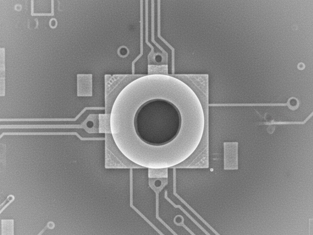
Voiding is the most common and studied defect. Voids form when gas—originating from flux volatiles, moisture, or entrained air—becomes trapped in molten solder. In larger joints, small voids are often inconsequential. In a micro-BGA joint, where a single large void can compromise the entire connection, even minor gas entrapment can cripple thermal conductivity and mechanical strength. Voids occupying more than 25% of a joint’s cross-sectional area are widely rejected; for micro-BGA, that threshold is met by voids barely visible to the naked eye.
Non-wetting is less common but more catastrophic. It occurs when molten solder fails to spread across the metallized pad, resulting in partial contact or complete dewetting. The cause is almost always inadequate oxide reduction at the solder-to-pad interface. The minimal flux volume in a micro-BGA joint and thermal imbalances can prevent the pad surface from being cleaned during the critical wetting window. The solder then beads up rather than spreading, creating a joint that may look intact but fails electrically or mechanically.
Bridging between adjacent balls is a volume control problem. Excessive solder paste, often from oversized apertures or poor stencil separation, causes adjacent deposits to merge during reflow. The fine pitch of micro-BGA packages—often 0.5 mm or less—offers little room for error. A paste deposit that spreads just 50 micrometers too far can create a bridge, resulting in a costly electrical short.
Insufficient solder volume is the inverse problem. Undersized paste deposits leave joints with inadequate fillet height or incomplete coverage of the ball-to-pad interface. These joints may pass initial inspection but are prone to fatigue failure under thermal cycling or mechanical stress. The defect is insidious, difficult to detect without X-ray imaging, and may not manifest until the product is in the field.
These four failure modes all hinge on process variables that operate at small scales and within narrow windows. High yields demand control over mechanisms that are either absent or negligible in larger solder joints.
Why Vacuum Reflow Eliminates the Root Cause
Atmospheric reflow operates at a fundamental disadvantage with micro-BGA. The pressure environment itself is the problem. At standard atmospheric pressure, gas generated by flux and moisture has nowhere to go once the solder melts and seals the pad. The surface tension of molten solder is too strong to allow gas bubbles to escape, particularly in such small volumes. The result is predictable: gas accumulates, forms voids, and solidifies in place. While process tweaks can reduce gas generation, they cannot eliminate the fundamental trapping mechanism.
Vacuum reflow removes the trap.
The Mechanism of Void Formation Under Atmospheric Pressure
Flux’s primary role is to reduce oxides on metal surfaces. This thermally activated reaction releases volatile organic compounds and water vapor, accelerating as the flux reaches its activation temperature (typically 150-180°C). In a conventional oven, these gases initially escape freely. The problem begins when solder particles coalesce into a liquid.
Once molten, the solder wets the pad and ball, forming a liquid bridge with high surface tension. Any gas still being generated is now trapped beneath this liquid layer. The gas cannot overcome the surface tension to escape, so it accumulates at the interface. As the assembly cools, these gas pockets freeze in place as voids. The small joint volume of a micro-BGA means even modest outgassing produces a high void percentage. Voids of 10-30% by volume are common in atmospheric reflow, even with low-voiding pastes.
How Vacuum Pressure Drives Outgassing Before Solidification
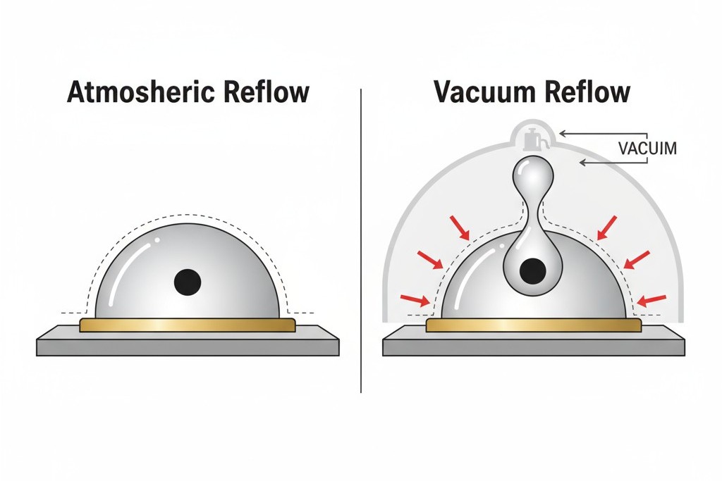
Vacuum reflow inverts the pressure gradient. By reducing the ambient pressure while the solder is molten, the process actively pulls gas out of the joint. Gas bubbles expand under the pressure differential, creating an outward force that helps them rise to the surface, rupture, and release their contents into the evacuated chamber. The surface tension barrier is overcome by the vacuum-induced pressure gradient.
The effectiveness depends on timing and pressure. A vacuum of 10 to 50 millibars is typical, creating a partial pressure high enough to drive rapid outgassing. This vacuum must be applied when the solder is fully molten but before solidification begins. Applied too early, it has little effect; too late, and the gas is already locked in. The optimal window is narrow, usually starting at or just below the solder’s liquidus temperature and lasting for 20 to 60 seconds.
The result is a dramatic, repeatable reduction in void content. Processes that produce 15-25% voiding under atmospheric reflow routinely achieve 2-5% under vacuum. With optimized paste and profiles, voiding below 1% is achievable.
This is not an incremental improvement. It is the elimination of the dominant failure mode in micro-BGA assembly.
Vacuum Reflow Profile Parameters for Micro-BGA
The reflow profile is a thermal roadmap that must also orchestrate the pressure environment. The profiles that deliver sub-one-percent voiding are designed around the assembly’s thermal response, the paste’s outgassing characteristics, and the vacuum system’s mechanical constraints.
Preheat and Soak Zone Strategy
The preheat zone brings the assembly to a uniform temperature and begins activating the flux. For micro-BGA, the ramp rate is typically limited to 1-3°C per second to prevent thermal shock. The soak zone, generally 60 to 120 seconds at 150-180°C, allows the flux to do the majority of its oxide reduction work, ensuring clean, wettable surfaces when the solder melts. Some profiles begin pulling a partial vacuum during the soak to preemptively remove volatiles, but this must be balanced against removing active flux components before their work is done.
Vacuum Application Timing and Pressure Targets
When and how deeply to apply vacuum defines the profile. Most commonly, the vacuum sequence begins at the end of the soak or the start of the ramp to peak temperature. The pressure is reduced gradually over 10 to 20 seconds to a target of 10 to 50 millibars. Lower pressures are more effective but increase the risk of volatilizing critical flux components. The vacuum is held throughout the time above liquidus—the critical window for void reduction, typically 30 to 60 seconds. As the assembly cools, the vacuum is released slowly over 10 to 30 seconds, allowing the solder to partially solidify before full atmospheric pressure is restored.
Peak Temperature and Cooling Rate Control
For standard SAC305 solder alloy (liquidus at 217°C), peak temperatures of 235-245°C are common, providing a sufficient margin to ensure uniform melting across the board. The time above liquidus (TAL) is a critical parameter, typically targeted for 30 to 60 seconds. Too short, and wetting may be incomplete; too long, and the intermetallic compound layers at the solder-pad interface grow excessively thick, leading to brittle joints. Achieving a uniform TAL across the assembly requires careful profiling with multiple thermocouples.
The cooling rate after peak temperature affects the solder’s grain structure. Faster cooling (2-4°C per second) produces finer grains, which are generally associated with improved mechanical properties. However, excessively fast cooling can cause thermal shock. A typical strategy involves a controlled rapid cool just after peak, followed by slower cooling as the solder solidifies.
Stencil and Aperture Design for Consistent Paste Deposits
Vacuum reflow is useless if the paste deposit is flawed. The print process is the foundation of micro-BGA yield, and for these components, stencil design is not a matter of scaling down standard practices.
Aperture Area Ratio and Release Efficiency
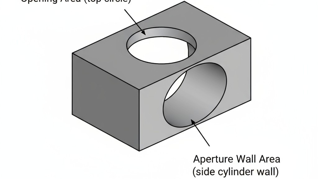
The aperture area ratio—the opening area divided by the aperture wall area—is the fundamental rule for predicting paste release. A ratio above 0.66 is the conventional guideline for ensuring paste deposits cleanly onto the pad instead of sticking to the aperture walls. For micro-BGA pads of 200-300 micrometers, this rule places severe constraints on stencil thickness.
Consider a 250-micrometer-diameter aperture. In a 100-micrometer-thick stencil, the area ratio is 0.62, just below the threshold. To achieve reliable release, the stencil must be thinned to around 90 micrometers. This illustrates the central trade-off: thinner stencils improve release but reduce paste volume, risking insufficient solder. The solution is a balanced design using the thinnest stencil compatible with the required solder volume.
Stencil Thickness Selection for Micro-BGA Pitch
Stencil thickness for micro-BGA is typically 75 to 125 micrometers, far thinner than the 150-200 micrometers used in standard SMT. For a 0.5 mm pitch, 100-125 micrometers is common; for a 0.4 mm pitch, this drops to 75-100 micrometers. The choice balances volume against release. At Bester PCBA, we use electroformed stencils for micro-BGA, with thickness selected based on pitch and paste type, as they offer superior wall geometry control compared to laser-cut stencils.
Aperture Shape and Wall Treatment
The ideal aperture is more than just a hole. For micro-BGA, rounded or chamfered corners prevent paste from tearing during stencil separation. A smooth wall finish is equally critical. Electropolishing aperture walls to a mirror finish reduces the adhesive force between the paste and stencil. Some stencils are further treated with paste-repellent nanocoatings, which can improve area ratio performance and allow for slightly thicker stencils or smaller apertures. Apertures may also be intentionally undersized by 5-10% relative to the pad to reduce paste volume and mitigate bridging on fine-pitch components.
Solder Paste Specifications for Wetting and Void Formation
The solder paste is the heart of the process. For micro-BGA, paste selection is a matter of matching material properties to the demands of small-volume joints formed under vacuum.
Particle Size Distribution and Type Classification
Type 3 paste (25-45 micrometer particles), common in general SMT, is too coarse for micro-BGA. The standard is Type 4 (20-38 micrometers) or Type 5 (15-25 micrometers). The finer powder flows more easily through small apertures, produces smoother deposits, and responds better to flux activation. Type 5 is preferred for pitches of 0.4 mm or tighter, where aperture sizes drop below 200 micrometers.
The trade-off with finer powder is sensitivity. The higher surface area increases the rate of oxidation during storage, which can degrade solderability. Type 5 paste has a shorter usable life and requires strict handling. Proper storage is non-negotiable; paste is tracked with lot control, kept refrigerated, and opened containers are discarded after the manufacturer’s recommended exposure period. This discipline is essential for consistent results.
Flux Activity and Wetting Performance
For micro-BGA, the flux is typically a no-clean formulation with moderate activity. No-clean fluxes leave benign residues, which is critical since cleaning dense micro-BGA sites is extremely difficult. The activity level must be sufficient to reduce oxides on pads and components but not so aggressive that it attacks metallization or generates excessive gas during reflow. Rosin-based and synthetic resin-based no-clean fluxes dominate this space, with modern synthetic resins often formulated for the lower outgassing required for vacuum reflow. Water-soluble fluxes are rarely used due to the risks associated with the mandatory, aggressive cleaning process.
Nitrogen Atmosphere as Oxidation Control
While vacuum reflow removes trapped gas, it doesn’t prevent oxidation on molten solder. A nitrogen atmosphere is the standard countermeasure. By displacing air and reducing oxygen concentration to below 100 parts per million, the oven environment dramatically slows the rate of oxide formation. The solder remains bright and metallic, and the flux is not burdened with removing freshly formed oxides.
For micro-BGA, the resulting improvement in wetting is invaluable. The small pads and solder volumes leave no margin for wetting degradation. Nitrogen provides a buffer, ensuring uniform wetting even on pads with less-than-perfect finishes. The key parameters are purity and flow rate, which are controlled to maintain a stable, low-oxygen environment without creating turbulence that could disturb paste deposits.
Process Integration and Measured Yield Outcomes
None of these techniques work in isolation. Vacuum reflow eliminates voids only if the paste deposit is correct. Stencil design controls volume only if the paste itself can release cleanly. Nitrogen prevents oxidation only if the reflow profile is correct. Achieving sub-one-percent defect rates depends on the disciplined integration of all these factors.

This requires diligent process validation. At Bester PCBA, every new micro-BGA design undergoes a manufacturability review. Initial builds are profiled with thermocouples, and the vacuum reflow profile is tuned to the board’s measured thermal response. First-article assemblies are X-rayed to assess voiding and identify the root cause of any defects.
The results validate the approach. Assemblies processed with this integrated system—optimized vacuum profiles, Type 4 or 5 paste, electroformed stencils, and a nitrogen atmosphere—consistently achieve void levels below 5% and total defect rates below 1% on micro-BGA joints. This is a repeatable, production-scale outcome. The defects that plague atmospheric reflow are effectively engineered out of the process.
The cost of this performance is discipline. Vacuum reflow equipment is more complex, fine-powder paste requires stricter handling, electroformed stencils cost more, and nitrogen is an operating expense. These are real trade-offs. The return is a process that builds in quality rather than inspecting for defects. For high-reliability applications where rework is impractical, the return justifies the investment.

