The sound of a drop test failure is distinct, but the silence that follows in the failure analysis lab is where the real tension lies. A prototype handheld device hits the concrete. The screen survives, the case survives, but the unit is dead. The immediate reflex in the engineering bullpens is to blame the fabrication house. The accusation is almost always the same: the laminate was “bad,” the resin was “undercured,” or the adhesion was “weak.”
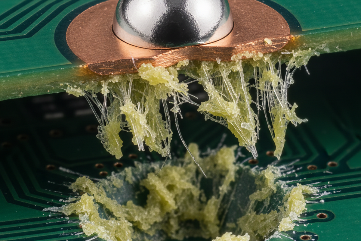
But when you zoom in on the cross-section, the story changes. The copper pad hasn’t just lifted; it has taken a chunk of the epoxy dielectric with it. This is pad cratering. It isn’t a failure of adhesion chemistry; it’s a failure of mechanical architecture. You cannot solve a geometry problem by demanding a “stronger” datasheet from your material supplier. If you see craters, you are likely asking the laminate to do a job that belongs to the mechanical chassis.
Anatomy of the Crater
You can’t fix the problem if you keep misidentifying it. Engineers often conflate any separation under a BGA (Ball Grid Array) with “pad lifting.” Pad lifting is usually a thermal phenomenon or a result of poor wetting during reflow. Pad cratering is a violent mechanical fracture.

Look at the failure site under a microscope. A true crater leaves a distinct divot in the laminate material itself. The copper pad is still firmly attached to the solder ball, and the solder ball is firmly attached to the component. The failure occurred entirely within the dielectric resin beneath the copper. It looks like a scoop of ice cream ripped out of the tub.
This distinction is critical because it rules out the common “Black Pad” panic. Black Pad is a chemical corrosion issue affecting ENIG (Electroless Nickel Immersion Gold) finishes, leaving a dark, planar surface where the solder failed to wet. If you see jagged epoxy and glass fibers sticking up from the board or attached to the bottom of the lifted pad, you do not have a Black Pad problem. You have a stress management problem. The resin didn’t fail chemically. It was mechanically overpowered.
The Physics of Speed: Strain Rate Sensitivity
The reason this failure mode is so insidious—and so often blamed on “bad batches”—is that FR-4 and similar laminates are strain-rate sensitive. A material that behaves with decent ductility during a slow thermal cycle or a static bend test will act like brittle glass during a high-speed impact.
When a device hits the ground, the shock wave travels through the PCB. If the board is allowed to flex, that strain energy has to go somewhere. In a standard drop event (following JEDEC JESD22-B111 or similar), the strain rate can be incredibly high. At these speeds, the polymer chains in the resin don’t have time to reorient and dissipate energy. They simply snap.
This is why looking at the Glass Transition Temperature (Tg) on a datasheet is a waste of time for this specific failure mode. Tg measures thermal performance, not fracture toughness (K1c) or high-speed modulus. You can pay a premium for high-Tg (170°C+) material and still see catastrophic cratering because the material is just as brittle, if not more so, at room temperature impact speeds.
The Silent Killers: It Happened Before the Drop

Before you even load the board into the drop tester, you may have already doomed the pads. A significant percentage of “drop test failures” are actually “depaneling failures” that just happened to finally open up during the drop.
Consider the mechanics of breaking a board out of a panel. If you use a V-score process and separate boards manually or with a pizza-cutter style blade, you introduce massive bending moments directly into the board edge. If a heavy connector or a BGA sits too close to that break line, the stress wave from the snap creates micro-cracks in the resin under the pads. These cracks are invisible to the naked eye and often pass electrical testing (ICT) because the copper is still touching. But the structural integrity of the resin is gone.
This is often where the “phantom” failures come from. The drop test didn’t break the resin; it just finished the job the router bit started. If you see cratering near the edges of the board, ignore the drop height for a moment and audit your depaneling station. Look for strain gauges on the fixture. If you don’t see them, you aren’t measuring the variable that is actually killing your yield.
The Solder Stiffness Trap
Many designers miss a counter-intuitive variable: making the solder joint stronger often makes the system weaker. The industry standard lead-free alloy, SAC305 (Sn-Ag-Cu), is widely used because it is reliable and well-understood. However, SAC305 has a relatively high Young’s Modulus—it is stiff.
In a drop event, you want compliance. You want something in the stack-up to act as a shock absorber. If the solder joint is stiff (SAC305), the component is stiff (ceramic BGA), and the copper pad is stiff, the only thing left to absorb the energy is the laminate resin. The resin is the “softest” thing in that specific high-stiffness chain, so it rips.
Switching to a lower-modulus alloy, like SAC105 or certain doped low-silver alloys, can drastically reduce cratering. These softer alloys deform plastically during the shock, absorbing the energy that would otherwise transfer into the laminate. It feels wrong to an engineer to ask for a “weaker” solder, but in the context of mechanical shock, compliance is survival. Of course, this introduces a trade-off: lower silver content often reduces thermal cycling reliability. You have to balance the risk of the device dying from a drop against the risk of it dying from thermal fatigue over five years. But for handheld devices, the drop is usually the primary killer.
Geometry is Destiny
Ultimately, you cannot cheat physics with a material spec. If you place a large, heavy BGA in the center of a thin PCB and then mount that PCB with screws only at the far corners, you have built a trampoline. When that trampoline flexes during a shock, the curvature is highest at the center—right where your BGA is soldered.
The most effective fix for pad cratering rarely involves a new laminate material. Usually, you just need a new mounting screw. Adding a standoff or a support boss near the large BGA increases the local stiffness of the board, preventing the flex that drives the crack. You are changing the mode shape of the board during vibration.
This applies to trace routing as well. While “trace tearing” is a cousin to cratering (where the copper trace snaps at the neck-down near the pad), the solution is similar. Teardrops and wider entry traces distribute the stress. But no amount of trace thickening will save a pad if the board is allowed to bow 4mm during an impact.
You must trace the force lines. Look at where the mass is (batteries, heat sinks, shields) and look at where the anchors are. If your sensitive components sit on the “fault lines” between these points, you are relying on the fracture toughness of a thin layer of epoxy to hold your product together. That is a gamble you will eventually lose. Secure the mass, stiffen the board locally, and stop hoping the resin will save you.
")


