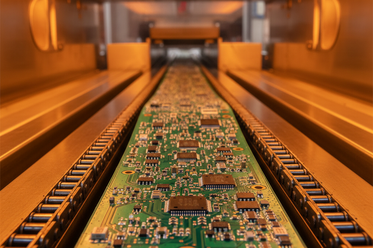
You are standing at the unloader of a 10-zone reflow oven, watching a 600mm LED strip or a long industrial controller board exit the tunnel. The middle of the board is visibly sagging, perhaps even scraping the mesh belt. Or worse, the board looks flat to the naked eye, but the functional test is failing. Connectors at the far ends have open pins, or center BGAs are showing open circuits.

The immediate instinct in most factories is to blame the thermal profile. The logic seems sound: if the solder isn’t wetting or joints are cracking, surely the oven settings are wrong. You call the process engineer. They attach a thermocouple, slow the belt speed to “soak it longer,” and bump the peak temperature up by 5°C.
This is the “Profile Trap.” It is the most common error in SMT troubleshooting for long form-factor assemblies.
If a board is physically warping—twisting like a potato chip or sagging like a hammock—no amount of air adjustment will fix it. You cannot profile your way out of gravity. You cannot use a “soak zone” to negotiate with the Coefficient of Thermal Expansion (CTE). When a long board fails only at the ends or the dead center, the oven profile is usually innocent. The culprit is mechanical.
The Bimetallic Strip Effect
To solve warpage, stop thinking about the board as an electrical interconnect and treat it as a mechanical laminate. A PCB is essentially a sandwich of fiberglass-reinforced epoxy (FR4) and copper foil. These two materials hate each other when heated.
FR4 expands at a specific rate (measured in ppm/°C). Copper expands at a different rate. On a long, narrow board, this mismatch creates massive internal stress. But the real trouble starts when the stack-up is unbalanced.
Consider a standard 4-layer board. If Layer 1 is covered in dense signal traces and Layer 4 is a solid copper ground pour, you have created a bimetallic strip. As the board ramps up to the 245°C peak reflow temperature, the side with more copper restricts expansion, while the resin-heavy side wants to grow. The result is a bow or twist.
This is distinct from “tombstoning,” where a small component like an 0402 stands up on one end. Unlike tombstoning, which is driven by wetting forces and uneven solder pull, warping is a structural failure where the substrate itself moves. If you see the board curling up at the corners, it isn’t a wetting problem; it’s the copper layout fighting the fiberglass, and the copper is winning.
Gravity and the Glass Transition
The second enemy is the material itself. Every FR4 laminate has a Glass Transition Temperature (Tg). Below this temperature, the resin is rigid and glass-like. Above it, the resin becomes soft, rubbery, and compliant.
For standard “High-Tg” materials, this transition happens around 170°C. However, SAC305 solder paste doesn’t even begin to melt until 217°C. This means that for the most critical part of the reflow process—the 60 to 90 seconds spent above liquidus—your circuit board is effectively a wet noodle.
If you run a 600mm long board that is only 1.0mm or 1.6mm thick, and you support it only by the edges on the conveyor rails, gravity takes over. The resin softens at 170°C, the board loses its structural rigidity, and the center collapses downward.
Engineers often try switching to low-temperature solder alloys (like BiSn, melting at 138°C) to avoid this. While that keeps you below the Tg of some materials, it introduces brittle joints and doesn’t solve the fundamental lack of stiffness. If the span is wide enough, gravity will defeat even a high-Tg material. The board will sag, center components will flood with solder or bridge, and connectors near the rail will twist inward.
The Invisible Crime Scene
The most frustrating part of warp-induced defects is that the evidence disappears by the time you see it.
When the board is inside the oven at 245°C, it might be bowed upward (frowning) by 2mm. In this state, a BGA component in the center might be lifted completely off its pads. The solder ball melts, but it hangs in mid-air, not touching the paste on the PCB. It oxidizes and forms a skin.
Then, as the board enters the cooling zone, the resin hardens again. The board snaps back to its original flat shape. The BGA ball drops down onto the pad, but it’s too late. The solder has already frozen. The ball rests on the pad like a head on a pillow. It makes physical contact, but creates no electrical bond.
This is the classic “Head-in-Pillow” (HiP) defect. At the test station, you press down on the chip and it passes. You let go, and it fails. X-ray looks fine because the ball shape is round. It is only when you perform destructive testing, like a “dye-and-pry” or cross-section analysis, that you see the microscopic gap. The defect happened at peak temperature, but the board looks innocent at room temperature.
Mechanical Cures (The Real Fix)
Since the problem is mechanical, the solution must be mechanical. You cannot fix a lack of stiffness with a soldering profile. You fix it by adding support.
The most effective solution for a sagging board is the Center Board Support (CBS). Most modern reflow ovens (from vendors like Heller, BTU, or Rehm) offer this option. It is a thin chain or a series of parking-brake-style pins that run down the exact center of the tunnel. It physically props up the middle of the board, preventing the sag.
If your oven lacks a CBS, or if bottom-side components prevent using a chain, you must use a reflow pallet.
A pallet is a fixture made of a composite material like Durostone or Ricocel. These materials are expensive—a custom fixture can run anywhere from $300 to $800 depending on complexity—but they are thermally stable. They do not warp at 260°C. You place the flimsy PCB inside the rigid pallet, and the pallet carries it through the oven flat.

Managers often balk at the cost. “It’s an added consumable,” they say. “It adds thermal mass, so we have to slow the line down.” This is true. But compare the cost of a $500 fixture to the cost of scrapping 20% of a production run of high-value industrial control boards. The ROI on a pallet is usually measured in days, not months.
Design Mitigations
If you are lucky enough to be involved before the board is laid out, you can fight the warp upstream. The most powerful tool in the designer’s kit is “copper thieving” or balancing.
Ensure the copper density is roughly symmetrical across the stack-up. If the top layer is 80% copper fill, the bottom layer should be similar. If you have a large open area with no traces, add a grid of floating copper squares (thieving) to balance the CTE stress. This prevents the bimetallic curling effect.
Even panelization plays a role. Leaving too much material on the breakaway rails can act as a stiffener—or a stressor, depending on the grain of the fiberglass.
The Verdict
When you see a long board failing at the ends or the center, stop the line. Do not touch the zone temperatures. Do not slow the belt speed.
Ask yourself: Is this board flat? Measure the bow. Look at the copper balance. Check the Tg rating of the laminate. If the board is bending, you need a fixture or a center support. Physics is undefeated in the SMT process. You have to support the board, because the resin certainly won’t support itself.

 Circuit Board Assembly")


