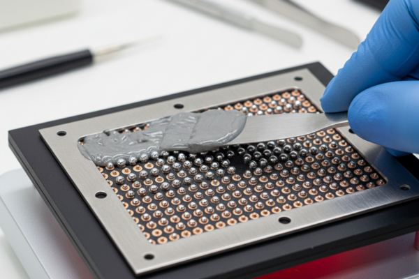
A conformal coat can look like a reliability win while behaving like a schedule threat. The classic failure mode isn’t dramatic: boards arrive “protected,” then ICT yield collapses because pogo pins stop making metal-to-metal contact through a thin film nobody thought mattered.
In one industrial sensor build (Q3 2021), acrylic with UV tracer was applied broadly. False-fails that used to sit around ~1–2% jumped to roughly ~11% until the test pad array was explicitly masked. On a ~500-unit lot, the hidden cost wasn’t the coating itself. It was the retest loop—about ~6 extra minutes per unit—plus the weekend work required to claw the ship date back.
That story isn’t really about acrylic versus urethane. It’s about how a process step changes the physics of test access. Under a 365 nm UV inspection light, the pads glowed the same way the rest of the board did, which is a polite way of saying “the thing that must be bare metal is not bare metal.” Once that happens, everybody wastes time blaming fixtures, firmware, operators, and “randomness,” because the board still looks fine.
There is a simple thesis that keeps teams out of that ditch: define keep-outs (test pads, connectors, RF zones) before arguing about chemistry; treat thickness as a variable you control; and insist on verification evidence. Then, add a rework plan that assumes the future will contain ECOs and repairs—because it will.
The Trap: “Protection” That Breaks the Board You Need to Diagnose
Selective coating is often framed as a reliability feature added late in the cycle, like a sticker that says “rugged.” That comfort story is expensive. The downstream pain shows up where people touch the board: bed-of-nails arrays, debug headers, board-to-board connectors, RF feed regions, and the rework bench.
A coating step that makes those touchpoints unreliable does not merely add friction; it creates false data. A coated test pad can turn a good solder joint into an ICT open, and now manufacturing is chasing ghosts. A connector cavity with a tiny meniscus of cured material can behave perfectly on the bench yet fail after vibration and a thermal cycle. That is exactly the sort of symptom that gets mislabeled as “firmware” or “intermittent harness.”
If the real question is “will coating ruin ICT?”, trust that instinct. It absolutely will if test access is treated as a verbal agreement instead of a requirement with a keep-out map and verification. The non-negotiable move is to explicitly call out “no coat on pads TP1–TP24” (or whatever the test array is) and then prove it—under UV if possible, or with a defined alternative. That isn’t pedantry; it’s test strategy.
The mainstream claim is that more coverage equals more reliability. The red-team view is that unverified coverage often equals less reliability, because it increases the chance of connector wicking, trapped contamination, and loss of diagnosability while leaving real vulnerabilities (shadowed edges, under-tall-component zones) untreated. The corrected framing is boring and effective: keep-outs + controlled thickness + verification + local reworkability.
Define the Sacred Keep-Outs Before Debating Chemistry
A practical way to start is to list the downstream touchpoints as if they are customers with veto power: ICT/bed-of-nails, functional test, debug probing, field service, and ECO rework. Each touchpoint has a failure mode that coatings can trigger. Pogo pins need bare metal. Debug probes need stable pads that won’t tear when a tech has to touch them twice. Field service needs connectors that don’t drift into “intermittent” after a few thermal cycles. Rework needs access that doesn’t require scraping for an hour just to see copper.
This list explains why “mask connectors” fails as a spec. Connectors are three-dimensional objects with cavities, capillary paths, and mating surfaces. In multiple RMA cycles (2018–2019), units returned with “won’t boot” tags but behaved fine until vibration and a thermal cycle pushed contact resistance over the edge. The root cause was conformal coat wicking into a board-to-board connector cavity—subtle enough that it wasn’t obvious without looking at the right angle, with the right light. Tape near the footprint had been treated as masking; it wasn’t.
The corrective action that moved the needle was physical exclusion: mating caps or plugs during coating, plus a hard keep-out boundary that operators could not “interpret.” That’s also a verification requirement: inspect connector cavities under UV at an angle, not from one straight-down glance.
RF zones are the other area where coating can be “beautiful” and still be wrong. In 2019, a telemetry product saw VSWR drift and a range drop on the order of ~20–30% in chamber A/B when urethane was applied around an RF can perimeter and antenna feed region. The fix wasn’t a moral stance against coating; it was an RF keep-out zone defined as a boundary on the drawing, then validated by comparing coated versus uncoated samples from the same lot. Coating can detune. Sometimes it doesn’t. The only honest answer is to treat it as a variable and prove it on that geometry, at that frequency.
Test pads, connectors, and RF zones are sacred. Everything else can be argued about.
And “sealed mystery boards” are not rugged. They’re just quiet until they aren’t.
Thickness and Coverage: The Hidden Variables
A lot of coating conversations stall out in chemistry names because chemistry feels like a decisive choice. In practice, two variables cause more real-world pain: where the coating ends up, and how thick it is where it matters. “Spray until it looks shiny” is a ritual, not a control plan. Gloss is not correlated with coverage under tall parts, along sharp edges, or near shadowed regions.
Shadowing is physical. Tall electrolytics, heat sinks, mezzanine connectors, and even standoffs create spray-angle occlusions. The board can look uniformly glossy from one view and still have an uncovered corrosion initiation line along an edge you never see. That is why a target thickness window matters: it forces the process to be repeatable and inspectable, and it keeps rework from becoming a demolition project. The actual number isn’t universal—thickness windows vary with chemistry, board geometry, and the failure mode being mitigated—so the safer posture is to define a target for the specific build and verify it rather than pretend one spec fits every assembly.
Verification is the divider between “we did coating” and “we have a coating process.” A vendor once claimed 100% coverage, and under 365 nm UV inspection with tracer, the truth showed up immediately: shadowing along tall components and under a mezzanine connector. This aligned uncomfortably well with where corrosion initiated on a returned unit. That kind of mismatch isn’t rare; it’s what happens when acceptance is based on appearance instead of evidence. Requiring before/after UV images per panel on the lot traveler isn’t glamorous, but it catches masking slips early—two in one 2023 run—before they become field narratives.
There is a recurring adjacent demand here: “we need full coverage.” Usually that phrase is fear wearing a technical hat because the environment spec is vague (“humidity,” “outdoors,” “industrial”) and the team wants certainty. The better version of that requirement is: define what must be protected (edges, specific high-impedance regions, exposed copper features), define what must remain accessible (test pads, connectors, RF), and define how coverage is proven (UV evidence, witness panels, or process coupons) on a pilot lot before scaling. Full coverage without proof is just full confidence.
Rework: The Part Everyone Pretends Won’t Happen
Rework isn’t a moral failure. It is production reality, especially in high-mix environments and any program where ECOs arrive after the build starts. In 2022, an ECO hit a power stage after roughly ~120 boards were already built. The boards had been coated with a tougher chemistry than usual because someone panicked about humidity, and the rework bench turned into a time sink. Under a microscope, a senior tech spent hours removing coating around MOSFETs and gate resistors without lifting solder mask. The work log made the cost visible: urethane-coated boards can take on the order of ~2–3× the rework time of acrylic when component replacement is needed. Most of that time isn’t soldering—it’s controlled removal.
If the question is “can we rework conformal coated PCBs?”, the practical answer is: only if the plan says how. The minimum viable rework plan is local removal, repair, local recoat, and re-verification (again, UV if that’s the scheme, or the agreed substitute). That plan belongs in the traveler as a defined step, not as tribal knowledge. Without it, a small defect becomes scrap, and a late ECO becomes a program-level crisis.
Heroic rework is a design-and-process failure, not a badge.
The useful pivot is that reworkability is created upstream by selective windows and keep-outs. A board can be well protected and still be serviceable if the coating boundaries are deliberate and repeatable.
Minimum Viable Spec: What to Hand a Coating House (and What to Demand Back)
The fastest way to tell whether a coating service is a process partner or a spray booth is the direction of their questions. A competent vendor won’t just ask “what coating do you want?” They will ask: “which nets do you still need to touch after coating?” That framing forces the conversation back to test pads, connectors, RF, and rework—exactly the places that create downstream cost.
A minimal spec doesn’t need to be long. It needs to be explicit about what must be true on the shop floor. A one-page masking diagram with keep-outs, allowed-overlap, a thickness target window, and inspection points can cut vendor back-and-forth dramatically (on the order of ~10 emails per ECO down to ~2 in one 2024 pattern) because it removes interpretation. Standard callouts like “no coat on pads TP1–TP24; 0.5 mm dam from pad edge” aren’t fussy; they prevent creeping coat that kills pogo reliability.
Here is what that “minimum viable spec” looks like as vendor-facing questions and acceptance demands (short on theory, heavy on evidence):
- Keep-outs: Where are the explicit keep-outs for test pads, debug headers (SWD/JTAG), and any bed-of-nails arrays, and how will the operator enforce them (tape, dots, boots, caps)?
- Connectors: What is the masking method? Tape near the footprint, or physical caps/plugs that block the cavity and mating surfaces?
- RF: What is the keep-out boundary (microstrip, antenna feed, SMA launch region), and how is it represented on the print or masking map?
- Thickness: What is the target thickness window for this build, and what spot checks or witness features verify it on this board geometry?
- Verification: Is it UV tracer inspection at 365 nm with defined viewing angles? If tracer is constrained, what substitute evidence is used (witness panels, process coupons, controlled spray parameters)?
- Coverage Definition: What does “100% coverage” mean operationally? Which faces, which edges, and how are shadowed zones addressed (spray path, fixturing, multiple angles)?
- Deliverables: What traveler artifacts will be delivered back (before/after UV photos per panel, signoffs, and any nonconformance notes)?
- Rework: What is the procedure to locally remove/recoat/re-verify without scrapping the assembly?
- Audit: What are the explicit exclusions around label areas, test fiducials, or masked witness features that let receiving inspection audit masking discipline quickly?
If those questions feel annoying, that is the point. They force the vendor to show process control instead of promising “fully protected.”
Verification artifacts belong in the traveler, not in an email thread. Requiring panel-level photos (UV if applicable) and defined signoff points is the mechanism that catches real masking slips before shipment. It also creates a feedback loop that makes FA and corrective actions concrete: “this boundary moved,” “this cap was missing,” “this shadow zone wasn’t hit,” instead of vague blame.
One more uncertainty has to be acknowledged: UV tracer is preferred because it is fast and unambiguous, but it isn’t universal. Some coatings or compliance constraints may limit tracer use. That does not remove the need to verify; it changes the method. Witness panels, process coupons, and controlled spray parameter documentation become the substitute evidence, and the spec should name that substitution explicitly rather than quietly hoping.
When Blanket Coating Actually Wins (and the Price You Still Pay)
There are environments where broader coverage is justified: continuous condensation, extreme corrosion exposure like salt fog profiles (teams may reference IEC 60068 families), and cases where the product is non-serviceable by design (sealed module, no field repair) and liability is high. In those scenarios, “selective by default” can bend because the downside of corrosion or leakage is larger than the downside of reduced access.
But blanket coating doesn’t get a pass on verification. If the board must be testable, test access has to be designed into the product (breakouts, test windows, bed-of-nails on the opposite side, protected pogo windows) and then enforced. If the board is not meant to be serviced, the manufacturing test strategy must be strong enough to compensate for the loss of downstream access, because once it is sealed, debugging becomes folklore.
A max-min framing helps: reduce the largest irreversible risks first. Irreversible risks include “can’t test it,” “can’t rework it,” and “can’t prove coverage on the edge that actually corrodes.” If blanket coating is mandated, treat it like a process that needs tighter verification, not like a reason to stop thinking about masking. Even in severe environments, connectors and RF zones often remain special cases that need explicit exclusion or controlled handling consistent with manufacturer guidance.
The field environment itself is often the most uncertain input. “Humidity” can mean intermittent condensation, washdown, salt exposure, or a customer requirement copied from a previous program. The antidote is to translate the words into scenarios and pass/fail evidence, then choose coverage that can be proven against those scenarios.
A Short Checklist That Prevents the Expensive Failures
- Define keep-outs first: test pads/ICT arrays, debug headers, connectors, RF feed and antenna regions.
- Make connector exclusion physical: caps/plugs for cavities and mating surfaces, not tape “near the connector.”
- Put the keep-outs on paper: a one-page masking map with boundaries and a few unambiguous callouts (e.g., dams from pad edges).
- Treat thickness as a controlled variable: set a target window and verify it on this board geometry (spot checks, witness features, or coupons).
- Choose a verification method and write it down: 365 nm UV inspection with tracer and defined viewing angles, or an explicit substitute if tracer is constrained.
- Require evidence artifacts: panel-level photos (before/after), traveler signoffs, and nonconformance notes tied to the map.
- Plan for shadowing: specify spray path/fixturing so tall parts and under-connector zones are addressed, not assumed.
- Write the rework loop into the traveler: local removal, repair, local recoat, re-verify.
- Run a pilot lot with an audit loop: coated vs uncoated (or masked vs unmasked) comparisons where risk is highest.
- Keep chemistry in its lane: select chemistry based on environment and rework reality, but do not let it replace masking discipline and proof.
The through-line is simple: selective coating that is verified is usually the reliability move because it protects what needs protection while preserving the ability to test, diagnose, and repair. The costs that destroy programs rarely come from coating material cost; they come from lost test coverage, connector intermittents, and rework time that explodes late.
Blanket coating can be the right call in severe environments. It just never earns the right to be unverified.


