The most dangerous sound in an RF manufacturing line is the one you can’t hear over the pick-and-place machines: the microscopic rattle of a solder bead, no larger than a grain of sand, rolling freely inside a sealed RF shield.

On the production line, this unit passes every electrical test. The Low Noise Amplifier (LNA) functions perfectly. The impedance matches. The board ships, gets installed in a telematics unit or automotive radar module, and goes out into the world. It looks like a “perfect” unit, right up until the vehicle hits a pothole or the temperature drops below freezing. Then, that tiny sphere of tin-silver-copper alloy shifts. It wedges itself between a 0201 capacitor and the shield wall, or bridges two pins on a QFN. The module dies instantly—or worse, it starts ghosting in and out of functionality.
This isn’t a theoretical failure mode. It’s a mechanical inevitability if your process relies on standard aperture designs for shielded areas. The mechanism is deceptive because it is rarely immediate. A loose bead can sit harmlessly in a “safe” area of the substrate for months. It requires energy to move into a kill position. In vibration testing, the bead might dance around without shorting anything. But in the field, the combination of vibration and thermal expansion creates a deterministic path to failure. The bead doesn’t just roll; it gets pushed.
You might assume a present bead will short immediately or not at all, but that simplifies the physics inside a sealed can too much. The environment under an RF shield is a distinct micro-climate where standard rules of solder surface tension and cleaning fluid dynamics do not apply. Treat the area under the shield like the rest of the board, and you are designing a time bomb.
The Thermal Pumping Station
These failures often spike after field deployment—specifically after winter/summer cycles—because of the Coefficient of Thermal Expansion (CTE) mismatch. You are dealing with a laminate board (FR4 or Rogers 4000 series), a metal shield frame (often nickel-silver or tin-plated steel), and the solder joints connecting them. These materials expand and contract at different rates. When a vehicle cycles from -40°C in a garage to +125°C under operating load, the shield frame flexes. It doesn’t just expand outwards; it warps and bows depending on the stamped geometry.
This flexing creates a pumping action. If a solder bead is trapped in the flux residue near the frame, the repeated expansion and contraction acts like a slow-motion broom. It nudges the bead, cycle by cycle, towards the path of least resistance. In a dense RF layout, that path often leads directly under a component standoff. We have seen cross-sections of returned units where a solder bead wasn’t just resting against a capacitor; the shield wall’s thermal movement had mechanically driven it underneath, crushing the bead into a flat conductive shim that shorted the terminals. The failure wasn’t random; the assembly physics pumped the bead into place.
Some reliability engineers try to solve this by freezing everything with underfill or staking compounds. They assume if they glue the components, the beads can’t move. This is often a mistake in high-frequency RF applications. Adding a staking compound changes the dielectric constant around your tuned circuits, detuning the filter or amplifier you are trying to protect. Furthermore, unless the underfill is perfectly void-free, the CTE mismatch between the epoxy and the shield can rip components off the pads during the same thermal cycles you are trying to survive. You cannot glue your way out of a process defect.
Ultimately, thermal expansion physics will always win against a loose conductive particle. If the bead exists inside the can, the probability of failure approaches 100% given enough time. The only valid reliability strategy is ensuring the bead never forms in the first place.
The Inspection Delusion
Manufacturing has a pervasive myth that you can inspect quality into a product. For under-can defects, this is objectively false. Do not rely on 2D X-ray or even 5DX (3D X-ray) to catch these beads reliably. An X-ray system struggles to distinguish between a solder bead resting harmlessly on the ground plane and one attached to the vertical wall of the shield can. Both look like dark circles in the grayscale image. If you tighten thresholds to catch every potential bead, your false call rate skyrockets, and operators start ignoring the machine. If you loosen them, you ship defects. The shield itself is a Faraday cage for light and a confusing artifact for X-rays.
Washing is equally ineffective. We often see process engineers crank up the pressure on inline aqueous cleaners, hoping to blast the beads out. But a reflowed solder bead is often held in place by tacky flux residue. To dislodge it, you need direct impingement of the cleaning fluid, which the RF shield prevents. The vent holes in a standard shield are designed for thermal venting, not fluid dynamics. High-pressure wash jets simply deflect off the can lid. Worse, the wash water can enter the can, dissolve some flux, and then fail to drain completely, leaving a pool of conductive soup that dries into dendritic growth later. You trade a hard short for a soft leakage current.
Occasionally, you will see a design using snap-on shield clips instead of a soldered frame. The argument is that you can wash and inspect the board before snapping the can on. While this solves the inspection problem, it introduces RF leakage issues and vibration risks that soldered frames do not have. If your RF performance requires a soldered frame, you must accept that you cannot wash or inspect the area underneath it effectively. You are flying blind.
The Aperture Diet: Stencil Design as the Only Fix
The root cause of solder beading under a shield is almost always excessive solder paste volume. The solution lies in the stencil aperture design, specifically in two areas: the large ground pads of the shield frame and the passive components nested inside.
When you print paste on a large ground pad for a shield frame, a 1:1 aperture opening is a disaster. During reflow, the heavy shield sinks into the molten solder. The displaced solder has to go somewhere. If it squeezes out vertically, it wets up the shield wall. If it squeezes out horizontally, it forms satellites—balls of solder that break away from the main fillet. These are your beads. To prevent this, you must aggressively reduce the paste volume. Never print 100% coverage on a shield ground pad.
The industry standard approach is the “home-plate” or “window-pane” reduction. You break the long linear pad into smaller segments, often reducing the total area of coverage to 50% or 60%. This gives the volatiles in the flux a path to escape (outgassing) without exploding the solder, and it provides a buffer zone for displaced molten solder to expand into without detaching from the main mass. If you are seeing beads, your first move should be to pull the Gerber files and check the aperture reduction. If it’s above 80%, you have found your problem.

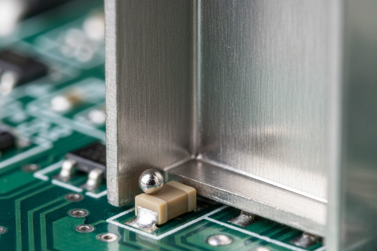
The second source is the “mid-chip” bead, which forms under the body of 0402 or 0201 chip components. This happens when the solder paste printed on the pads slumps or is squished under the component body during placement. When it reflows, capillary action pulls the solder to the center, where it coalesces into a hidden bead. Under a shield, this is fatal because the bead is trapped. The fix here is using the “home-plate” aperture shape for the component pads themselves—removing paste from the inner edge of the pad to prevent it from flowing under the component.
Don’t confuse actual solder beads with flux residue accumulation. RF engineers often panic when they see VSWR drift and blame “contamination.” Flux residue is inevitable in a no-clean process. It changes the dielectric properties slightly, but unlike a solder bead, it isn’t a conductive short. Do not let the team conflate the two. You can tune a circuit to account for flux residue; you cannot tune it to account for a loose metal ball.
Implementing these stencil changes is cheap. A new stencil costs a few hundred dollars. Reworking a thousand units where you have to use a hot air station to lift a soldered shield—cooking the neighboring components and destroying the PCB pads in the process—costs tens of thousands. The math is brutal and simple. You pay for the stencil design, or you pay for the scrap.
The Unforgiving Geometry
Finally, respect the physical limitations of the assembly process during the layout phase. Designers often place capacitors or resistors within 0.2mm of the shield wall to save space. This is malpractice. When the shield frame is placed, any slight misalignment or skew in the pick-and-place machine can cause the frame to land on the component pad or the component itself. Even if it clears, the proximity creates a “flux trap” where capillary forces can draw solder from the component pad onto the shield wall, creating a bridge.
There is no magical reflow profile that fixes bad geometry. You can tweak the soak time to activate the flux gently, and you can adjust the peak temperature to minimize slump, but these are marginal gains. If your stencil is printing too much paste, or your components are too close to the shield, surface tension physics will create beads. The only way to guarantee a reliable RF module is to starve the joint of excess solder and give the process room to breathe.


