There is a pervasive superstition in power electronics manufacturing that equates a beautiful X-ray image with a reliable part. You see it on production lines from Shenzhen to Guadalajara: a quality manager holding up a batch of QFNs because the voiding percentage hit 28% instead of the arbitrary 25% dictated by IPC-A-610. Meanwhile, the line stops, the “bad” boards are scrapped or reworked, and everyone pats themselves on the back for catching a defect.
That isn’t reliability engineering. It’s a beauty contest.
Physics doesn’t care about your gray-scale thresholds. Physics only cares about the thermal path from the junction to the ambient environment. If you prioritize void percentage over void location, you’re likely scrapping good hardware while letting dangerous parts slip right through the gate.
The problem is that we’ve allowed workmanship standards—which are excellent for determining if a process is drifting—to masquerade as reliability physics. A standard like IPC-A-610 Class 3 is a binary pass/fail gauge designed for contract disputes and visual consistency, not for predicting whether a MOSFET will survive a ten-year duty cycle in an automotive traction inverter.
When you treat a 25% void limit as a hard cliff for thermal failure, you ignore the concept of the “Thermal Budget.” A part with 30% voiding might have a Junction-to-Case thermal resistance (Rth-jc) that is statistically identical to a part with 10% voiding, depending entirely on where those voids sit. We need to stop auditing shadows and start engineering the heat flow.
Geography Over Geometry
Heat flows like water, taking the path of least resistance, and it doesn’t flow uniformly across the entire die attach paddle.

Take a high-power 5×6 PowerQFN. In testing, you might encounter a unit with massive voiding—pushing 45%—caused by aggressive flux outgassing. To the naked eye of an X-ray machine, it looks like a disaster, a Swiss cheese of solder that should burn up instantly. But if you map those voids, you often find they are “champagne bubbles” clustered entirely around the perimeter of the pad, driven there by wetting forces during reflow. The center of the pad, directly underneath the silicon die’s active hotspot, is solid.
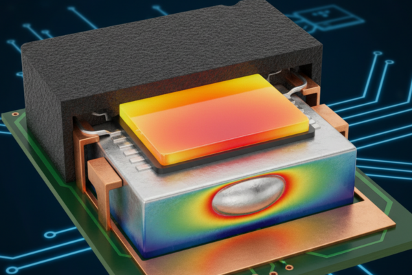
When you run this “failed” part on a dynode bench with a thermocouple or a transient thermal tester, the result is often shocking: the junction temperature (Tj) rise is within 2°C of a “perfect” control unit. The heat generated at the die center has a direct, uninterrupted copper path to the leadframe. The peripheral voids are thermally irrelevant because the heat never needed to travel through those edges to escape.
Conversely, you can have a part with only 8% total voiding—a “pass” by any standard—where that single void is a large bubble trapped directly under the die’s hotspot. That localized insulation creates a massive thermal bottleneck, leading to current crowding and a rapid spike in Tj that no datasheet margin can cover. The percentage is low, but the reliability risk is critical.
This is where the industry’s obsession with simple numbers fails. The relationship between void percentage and thermal resistance isn’t linear; it is geometric and highly dependent on the specific package architecture (e.g., LFPAK vs. D2PAK).
It’s tempting to look for a magic bullet like silver sintering to solve this, assuming that a denser, void-free material will fix the issue. But while sintering offers higher thermal conductivity, it introduces its own demons, particularly around interface delamination on large-area dies. If you switch materials without understanding the geography of your heat flow, you are just trading one failure mode for a more expensive one.
The Zero-Void Paradox
There is a darker side to the pursuit of the “perfect” solder joint, one that often blindsides teams dealing with harsh thermal cycling (-40°C to 125°C).
I’ve analyzed field returns of high-reliability traction modules where the X-ray inspection data from the factory showed near-zero voiding on the DBC (Direct Bonded Copper) substrates. They looked flawless. Yet, in the field, the solder joints cracked and fatigued prematurely. The investigation revealed that the lack of voids was actually a symptom of a bondline that was too thin.
In the rush to eliminate voids, the process had been tuned to squeeze the package down tight, leaving almost no solder standoff height to act as a mechanical buffer. Solder is a compliant material; it needs volume to absorb the coefficient of thermal expansion (CTE) mismatch between the stiff silicon/leadframe and the PCB.
When you achieve “zero voids” by crushing the bondline, you remove that stress relief. A small amount of distributed voiding can actually arrest crack propagation, acting as a stress break in the lattice. A perfectly solid, microscopically thin joint transfers all that mechanical stress directly to the intermetallic layers, leading to fatigue cracks that sever the thermal path far faster than a few bubbles ever would. Zero isn’t the goal; often, a perfect zero-void joint is just a brittle failure waiting to happen.
Stop Guessing, Start Measuring
If you can’t rely on X-ray percentage, how do you validate the process? You have to stop looking at 2D shadows and start measuring the dynamic thermal response. Static thermal resistance (Rth) is useful, but Transient Thermal Impedance (Zth) is the truth-teller. Using methods outlined in JEDEC JESD51-14, specifically the dual-interface method, allows you to see the heat propagation through the stackup in time.
By analyzing the structure function curve generated by a T3Ster or similar equipment, you can pinpoint exactly where the thermal bottleneck is occurring. You can distinguish between a void at the die-attach interface and a delamination at the copper-to-FR4 layer. This is the only way to prove whether a void is “insulating” (blocking the path) or “irrelevant” (sitting in a dead zone).
It requires investment in lab equipment and the patience to interpret complex curves, but it moves the conversation from “this looks ugly” to “this runs 15°C hotter.” That is data you can take to a client or a compliance officer to justify a deviation from the standard specs.
Engineering the Exit

Before you go asking management for half a million dollars to buy a vacuum reflow oven to crush your void numbers, look at your stencil design. Vacuum reflow is a powerful tool, but it is often used as a crutch for poor process engineering. The most common cause of voiding in large thermal pads is simple gas entrapment—volatiles from the flux have nowhere to go during the soak phase.
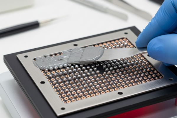
Often, you can reduce voiding from a failing 35% to a passing 15% simply by changing the aperture design from a single large block to a “window-pane” grid. This creates channels for the outgassing flux to escape before the solder goes liquidus. Combine this with a profile optimization—tweak the soak time to ensure full volatile activation—and you can often solve the problem for the cost of a new stencil ($300) rather than a new oven ($500k).
Ultimately, your goal is to write a process specification that reflects reality. Don’t copy-paste the IPC Class 3 limits into your master drawing unless you enjoy arguing with your contract manufacturer. Define your criteria based on the physics of your specific power density:
- Define Critical Zones: Specify that voids under the die thermal pad (the hotspot) are weighted more heavily than peripheral voids.
- Mandate Bondline Control: Set minimum standoff heights to prevent stress failures.
- Use Zth for Verification: Qualify the process using thermal transient testing, then use X-ray only as a process monitor to ensure nothing drifts.
Reliability is about ensuring the device works, not polishing X-rays for a stock photo.


