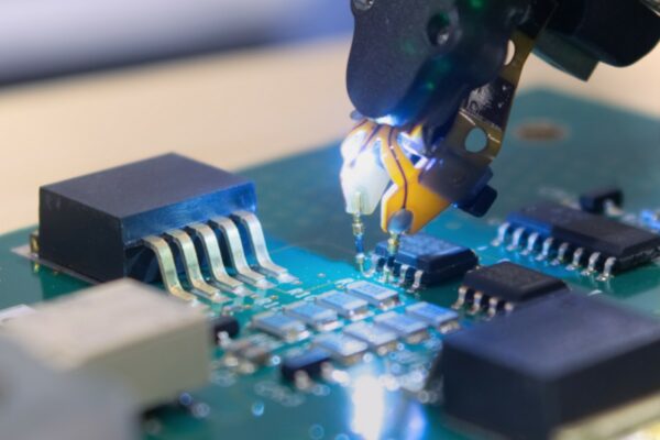
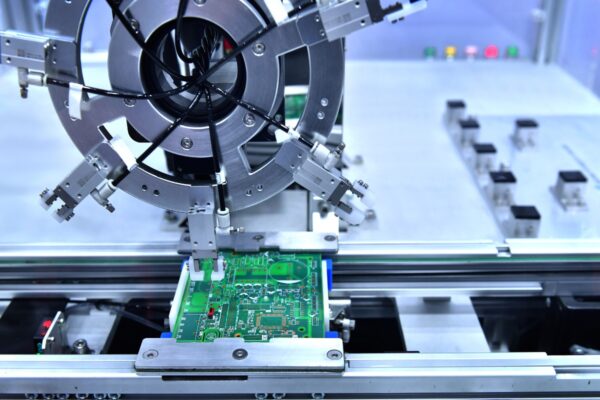
Automated optical inspection (AOI) is the cornerstone of quality assurance in modern electronics assembly. Its dominance, however, rests on a fragile assumption: that the camera can see what it needs to judge. When design trends collide with optical physics, that assumption shatters. Matte-black solder masks, prized for their sleek appearance, absorb the very light that AOI systems need for contrast. Simultaneously, the relentless miniaturization of passive components has pushed 01005 parts to the edge of what even high-resolution cameras can reliably resolve. The result is a quality control crisis, defined by false positives that scrap good boards and false negatives that allow defects to escape into the field.
The common instinct is to tune the AOI system more aggressively—tightening thresholds, adjusting lighting angles. This reaction fundamentally misunderstands the problem. The issue isn’t one of calibration; it’s one of physics. A dark mask simply doesn’t reflect enough light to create the grayscale gradient an algorithm needs to distinguish a pad from a trace. An 01005 resistor occupies too few pixels for reliable edge detection. No amount of software tweaking can extract a signal that isn’t there. The solution lies in adopting inspection methods that bypass the optical contrast problem entirely: 3D solder paste inspection, which measures topology instead of reflectance, and automated X-ray inspection, which penetrates the assembly to reveal hidden solder joints. For manufacturers committed to dark cosmetics or ultra-fine-pitch density, a multi-method inspection strategy is not an enhancement. It is a necessity.
The Optical Contrast Problem: Why Dark Masks and Tiny Passives Break AOI
Automated optical inspection works by analyzing variations in grayscale intensity. The system thrives on strong visual contrast between elements—bright solder against a green mask, dark component bodies against white silkscreen. When that contrast collapses, the algorithm loses its reference frame. Two of the most common culprits, matte-black solder masks and 01005 passive components, each present a distinct but equally disruptive challenge.
Matte-Black Masks and the Light Absorption Barrier
The aesthetic appeal of matte-black solder masks has made them a standard in premium consumer electronics, but their optical properties create a hostile environment for reflected light inspection. A black mask swallows most incident light rather than reflecting it. What little light does return is scattered diffusely by the matte texture, eliminating the sharp highlights that cameras use to identify pad edges and trace boundaries. The resulting image is a low-contrast wash where solder joints, copper pads, and the surrounding mask blend into a narrow band of gray.
AOI algorithms depend on sharp transitions in pixel intensity to perform edge detection. When a solder fillet on a black mask reflects only marginally more light than the mask itself, the gradient is too shallow for the system to make a confident call. This forces a choice between two poor options: raise the sensitivity and flag countless false defects, or lower it and miss real problems like solder bridges or insufficient wetting. In a production environment where yield and quality are measured in basis points, neither is acceptable.
01005 Components at the Resolution Threshold
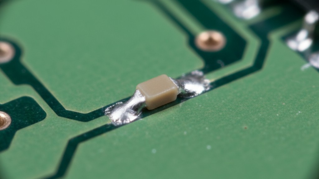
The 01005 passive component measures a mere 0.4 by 0.2 millimeters, a footprint so small it challenges the spatial resolution of standard AOI cameras. At typical working distances, an 01005 component may occupy fewer than ten pixels in each dimension—well below the threshold required for robust shape analysis. Edge detection algorithms need a clear boundary of pixels to determine if a component is present, correctly oriented, and properly centered. When the entire part spans only a handful of pixels, the signal-to-noise ratio plummets.
Compounding this is the contrast problem. 01005 resistors and capacitors are often black or dark brown, offering minimal intensity difference against a dark mask. The component’s tiny size means any slight variation in lighting can push its few reflective pixels below the detection threshold or drown them in noise from adjacent silkscreen or traces. The camera no longer sees a distinct object. It sees a noisy patch of pixels that may or may not be a component, leading to high reject rates.
The False Call Dilemma: Escapes vs. Overkill
Low optical contrast forces a painful trade-off between two types of error, each with direct production costs. When an AOI system operates on marginal signal quality, it can be tuned to be aggressive or lenient, creating a dilemma between catching more defects at the expense of yield, or preserving yield at the expense of quality.
False positives occur when the AOI flags a good assembly for rework. In high-volume production, a false positive rate of even two percent removes thousands of perfectly good boards from the line for manual inspection. Each false call consumes labor, slows throughput, and erodes confidence in the system. Eventually, operators begin to ignore AOI alerts, assuming they are noise. This learned distrust is dangerous, conditioning the production floor to bypass its own quality gates.
False negatives, or escapes, are the opposite failure: a defective assembly that the AOI passes as good. The cost of an escape scales dramatically the later it is caught. A defect found in functional test is expensive; a defect that reaches the field triggers warranty claims, recalls, and reputational damage. In high-reliability or safety-critical applications, a single escape can be catastrophic. The fear of escapes is what drives manufacturers to tune AOI systems aggressively, which circles right back to the false positive problem.
This is the tuning paradox: lowering the detection threshold to catch more defects kills yield with false positives. Raising the threshold to reduce overkill allows more defects to escape. With good optical contrast, this trade-off is manageable because the signal is strong. On dark masks or 01005 assemblies, the uncertainty is so wide that no threshold setting can deliver both acceptable yield and defect capture. The system is being asked to make reliable decisions from unreliable data. When the data itself is flawed, the only solution is to change the data source.
3D Solder Paste Inspection: The First Line of Defense
The limitations of grayscale imaging have driven the adoption of 3D solder paste inspection (SPI). Unlike AOI, which analyzes reflected light, 3D SPI measures the physical topology of solder paste deposits before component placement. This shifts the inspection from a subjective “Does this look correct?” to a quantitative “Is the correct volume of paste in the correct location?” That question is more precise and fundamentally immune to mask color.
Height Mapping vs. Grayscale Imaging
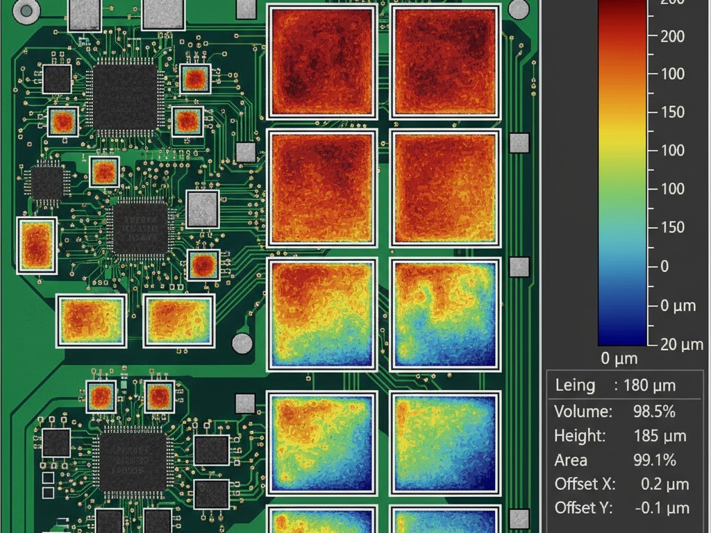
Three-dimensional SPI systems use structured light or lasers to build a detailed height map of the stencil-printed solder paste. Every pad is measured for paste volume, height, area, and offset. These metrics are derived from physical geometry, not pixel intensity. A dark mask doesn’t absorb a laser line or distort a projected grid the way it absorbs white light. The reflective, three-dimensional paste generates a clear topological signature regardless of the substrate beneath it.
This precision is critical because most post-reflow defects—insufficient solder, bridging, tombstoning—begin as paste deposition errors. A pad with only 70 percent of the required paste volume will likely produce a weak joint, even with perfect component placement. By catching these problems before components are even placed, 3D SPI prevents defects from moving downstream where they become exponentially harder and more expensive to find and fix. It turns a defect lottery into a controlled process.
The height map also enables confident inspection of 01005 paste deposits. While the deposit is small, it is large enough to generate a measurable height profile. The system can verify not just presence but correct volume and centering, providing a quantitative pass-fail criterion that doesn’t rely on pixel counting. This makes 3D SPI essential for any assembly combining ultra-small passives with challenging mask colors.
Automated X-Ray Inspection for Post-Reflow Verification
While 3D SPI masters pre-reflow quality, it cannot assess the final solder joint after reflow. For that, automated X-ray inspection (AXI) is required. AXI uses penetrating radiation to image the internal structure of solder connections, bypassing surface visibility problems entirely. It is indifferent to mask color, component size, or whether a joint is hidden under a package. AXI evaluates the solder itself, making it indispensable for modern high-density assemblies.
Seeing Through the Board: BGAs and Hidden Joints
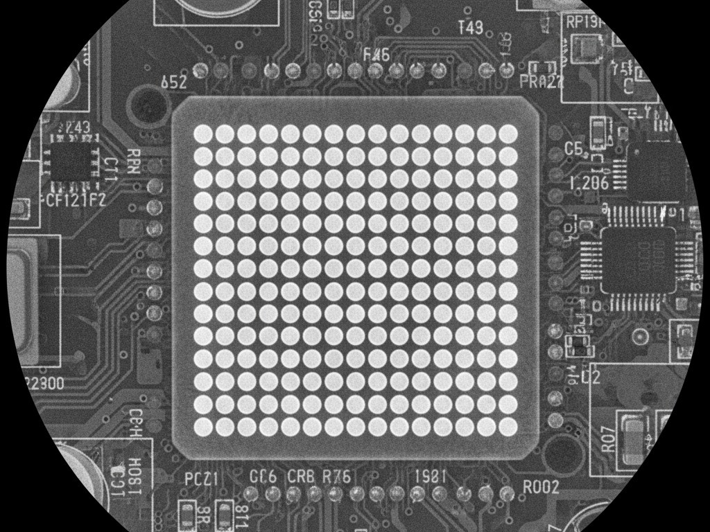
Ball grid arrays (BGAs) and other area-array packages present a geometric impossibility for optical inspection: their solder joints are completely hidden. No camera can reveal a voided or missing solder ball under a BGA. X-ray inspection solves this by transmitting radiation through the assembly. Solder, being dense, absorbs more radiation and appears as a distinct feature, allowing the system to verify ball presence, shape, and voiding.
On assemblies with dark masks, AXI provides another crucial benefit: it can inspect peripheral joints on QFNs and other packages without relying on optical contrast. The X-ray image reveals the solder mass directly, exposing issues like insufficient wetting, bridging, or head-in-pillow defects that would be ambiguous or invisible to a camera. This makes AXI not just a necessity for area-array packages but a powerful complement to AOI on any assembly where contrast is poor.
The trade-off is speed and cost. X-ray systems are slower than optical cameras and represent a significant capital investment. For this reason, AXI is typically deployed selectively on high-risk zones like BGA fields. On assemblies populated with dark masks and dense BGAs, this targeted approach is non-negotiable. The escapes AXI prevents are precisely the defects most likely to pass optical inspection and cause catastrophic field failures.
Process Adjustments to Raise Yield
Not every manufacturer can immediately invest in new 3D SPI and AXI lines. In these cases, rigorous process-level adjustments can reduce defect rates and improve the performance of existing AOI systems, even if they can’t fully replace advanced inspection technologies. The goal is to tighten the process window, reducing the variance that creates defects in the first place.
Stencil aperture optimization. The volume and shape of solder paste deposits have an outsized influence on joint quality. For fine-pitch components, laser-cut stencils with electropolished walls and optimized aperture geometries improve paste release and consistency. Reducing paste variability means fewer marginal assemblies fall into AOI’s uncertainty band.
Component placement accuracy. Tombstoning and misalignment on small passives often result from placement offsets. High-precision pick-and-place systems with vision-based correction can center 01005 components more reliably, preventing the solder wicking imbalances that cause such defects. This doesn’t solve the visibility problem, but a lower defect rate means fewer escapes.
Mask color compromise. Sometimes, the aesthetic requirement for matte-black can be relaxed to a dark green or dark blue variant. While still challenging, these colors can provide marginally better optical contrast, potentially shifting AOI performance from unusable to barely adequate for certain product lines. This is a design trade-off that balances inspection reliability against cosmetic preference.
These adjustments are valuable but limited. A well-optimized process will still produce occasional defects, and those defects will still be difficult to see on dark masks. Process discipline buys margin, but it does not change the physics of light absorption.
Building a Multi-Method Inspection Strategy
No single inspection technology is sufficient for modern assemblies that combine dark solder masks, ultra-small components, and area-array packages. The solution is a layered strategy that deploys the right technology at the right process step, matching the strength of each method to the specific failure modes it is designed to catch.
A robust strategy begins with 3D solder paste inspection before component placement. This catches paste volume, offset, and bridging defects at the earliest possible point. For assemblies with 01005 components or fine-pitch devices, 3D SPI is the only reliable way to verify the foundation of a good solder joint.
After reflow, automated X-ray inspection should be targeted at BGA zones and other hidden joints. AXI is used selectively on high-value or high-risk assemblies where the cost of a field failure from an escape far exceeds the cost of inspection. This requires clear criteria for which boards or zones demand X-ray coverage to avoid bottlenecking production.
Post-reflow AOI still has a role, but it must be deployed intelligently. On assemblies with dark masks, AOI should focus on larger components, leaded packages, and areas where optical contrast remains adequate. It is repositioned as one tool among several, inspecting what it can reliably see while leaving the most challenging zones to other methods. This means programming the AOI to de-emphasize or skip 01005 fields on black masks to prevent the flood of false positives that erodes operator trust.
The goal is not to inspect quality into the product, but to build quality into the process and use inspection to verify it. On assemblies where optical physics makes traditional AOI unreliable, that verification requires a combination of methods. This is the baseline requirement for delivering reliable products when design trends outpace the capabilities of any single inspection technology.
