The most expensive silence in electronics manufacturing is the one that follows a successful functional test, only to be broken six months later by a field report. A fleet tracker mounted to a truck chassis in Detroit stops reporting its position. A smart meter in a basement goes intermittent. The 8D report eventually lands on a desk, and the root cause is almost always the same: a cracked solder joint on a castellated module.
These failures are rarely electrical. The silicon inside the Bluetooth or GPS module is fine. The failure is mechanical, usually baked into the design long before the first stencil is cut. When you integrate a pre-certified module—whether it’s a u-blox GPS or an Espressif WiFi unit—you are bolting a rigid block onto a flexible FR4 substrate. If that connection relies on the bare minimum solder pads recommended in the datasheet, you are building a product that will pass factory burn-in but fail the first time it hits a pothole or a thermal cycle.
Forget “bad solder batches” or operator error; this is a geometry problem. The physics of a castellated joint are unforgiving and behave differently than standard surface mount components. During the prototype phase, these modules are often hand-soldered. A technician floods the joint with wire solder, creating a massive, robust fillet that wraps around the castellation. The prototype works perfectly on the bench. But when that design moves to volume production, the solder volume is dictated by a 5-mil laser-cut stencil. The resulting joint is a fraction of the size, and suddenly, the mechanical redundancy is gone. If the pad geometry wasn’t designed for that lean production reality, the joint will starve, stress, and eventually shear.
The Datasheet is a Marketing Document
You have to accept that the “Recommended Land Pattern” in a module’s datasheet is not an engineering truth—it is a compromise. Module vendors are incentivized to minimize the footprint of their device to make it attractive to designers fighting for board real estate. They show you a pad extension that is just enough to get an electrical connection in a static environment. They do not optimize for high-vibration environments or IPC Class 3 reliability.
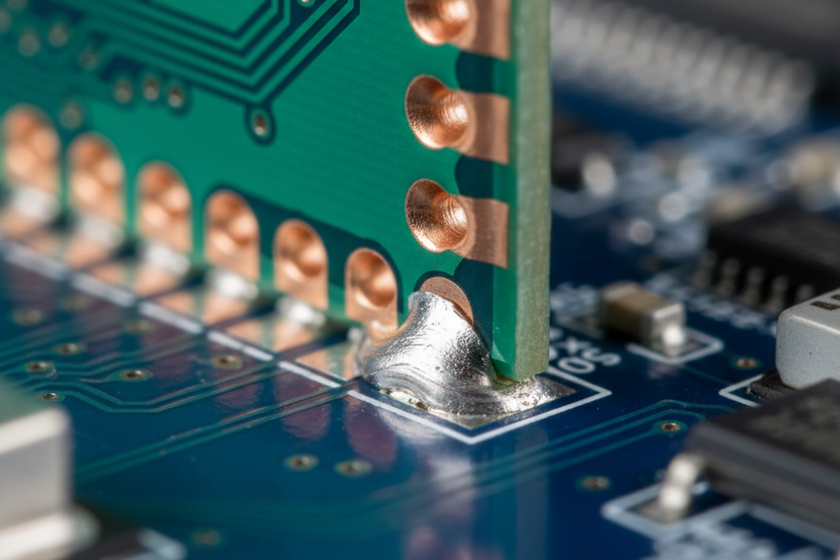
For a reliable castellated joint, ignore the vendor’s suggestion of a 0.8mm pad extension. Push for something closer to 1.2mm or even 1.5mm. This extra copper is not wasted space; it is the foundation for the “Heel Fillet.”
Most visual inspection criteria (like standard AOI) focus on the “Toe Fillet”—the shiny slope of solder visible on the outside of the module. But the Toe takes very little load. The structural integrity of a castellated joint lives in the Heel—the solder that wicks underneath the module and up the inner wall of the castellation. This is where the shear forces from board flex and thermal expansion concentrate. If your pad stops flush with the module edge, or only extends slightly, you get zero Heel fillet. You get a “butt joint” that is incredibly weak in shear. By extending the pad outward, you allow the solder paste to wet properly and flow back under the castellation, creating a meniscus that can actually absorb vibration energy.

Mechanical engineers often try to fix this geometry problem with chemistry—specifically, underfill or conformal coating. “Can’t we just glue it down?” is a common refrain when space is tight. While underfill adds rigidity, it makes rework a nightmare. If a module fails a functional test and is glued to the board, you are often scrapping the entire PCBA. Chemistry is not a substitute for geometry. Design the pads correctly, and you won’t need the glue.
Aperture Control: The Hidden Short
Once the pads are large enough to support a joint, the risk vector shifts to the stencil. A common disaster scenario involves a WiFi module with a metal RF shield. The designer lays out the footprint, and the stencil shop cuts a standard 1:1 aperture for the pads.
In production, the solder paste prints, the board enters the reflow oven, and the paste slumps as it heats up. Because castellated pads are often large and rectangular, that slump can bridge the tiny gap between a ground pad and a VCC pad. If this bridging happens underneath the metal shield of the module, it is invisible to AOI (Automated Optical Inspection). You won’t find it until the unit draws excessive current at the test station.
We have seen production runs where 30% of the boards required rework because of this hidden bridging. The fix is a rigorous reduction in stencil aperture. You do not need 100% paste coverage on these large pads. A reduction to 80% or even 70%—specifically pulling back the aperture from the inner edge under the module—is critical. This prevents the “solder balling” and bridging that occurs where you can’t see it.
This is particularly volatile if you are using water-soluble flux, which can get trapped under the module and cause dendritic growth later. However, even with no-clean chemistries, the physical bridge is the immediate killer. The goal is to starve the inner edge slightly to prevent bridging while flooding the outer extension to build that critical fillet.
The Mechanical Environment

Beyond the solder and the stencil, the module’s physical location on the board dictates its survival. A castellated module is effectively a rigid ceramic or stiff FR4 brick sitting on a flexible mainboard. When that mainboard flexes—whether from thermal expansion, vibration, or the violence of depanelization—the stress creates a shear moment at the solder joints.
The most dangerous operation in the life of a castellated module is often the moment the board is separated from the panel. If a heavy module is placed within 10mm of a V-score line, the “snap” of the pizza-cutter depaneler sends a shockwave through the fiberglass. We have seen cross-sections where the copper pad was literally torn off the FR4 laminate before the device ever left the factory.
If the product is destined for a high-vibration environment—think automotive telematics, industrial robotics, or anything mounted to a motor—placement is even more critical. Avoid the center of the board where “drum-skinning” (oscillation) is worst. Place modules near mounting screws where the board is stiffest.
If you cannot move the module, cannot extend the pads, and cannot change the stencil, you are left with a product that is essentially a ticking clock. No amount of process tweaking at the SMT line can compensate for a component that is mechanically fighting the board it is soldered to. The only real fix is to respect the physics of the joint: give it copper to grip, keep it away from the bending edges, and inspect the heel, not just the toe.


 Circuit Board Assembly")

