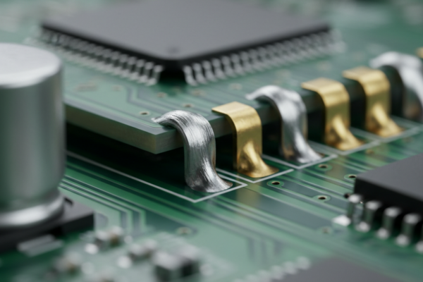
The difference between a functional module and a scrapped prototype often comes down to the microscopic edge of the board. When a shipment of daughterboards arrives, the first inspection step shouldn’t be a continuity test; it should be a visual check under a 30x loupe. If the edge plating looks like it has been chewed by a dull animal, the board is already compromised. A “burr” in this context isn’t merely cosmetic. It is a structural hazard—a sliver of copper, torn from the substrate, waiting to bridge two pads or lift entirely during reflow.

This failure mode rarely results from “bad luck” or a “bad batch” of laminate. Almost always, it is a failure of geometry and instruction. Designers often assume that placing a via on the board outline in their CAD tool—be it Altium, KiCad, or Eagle—is sufficient to generate a castellation. It is not. While the CAD screen shows a perfect semi-circle, the factory floor reality involves a high-speed steel router bit exerting significant torque on a thin foil of copper barely glued to the fiberglass weave. If that copper isn’t mechanically anchored, or if the router bit enters at the wrong angle, the plating will tear.
This tearing drives solder bridging during assembly. If the edge is ragged, the solder paste has a wick to travel along, connecting adjacent pads meant to remain isolated. Solving the mechanical cut solves the electrical short.
The Physics of the Tear
To design a robust castellation, you must visualize the toolpath. A standard PCB router bit—often 2.0mm or 2.4mm in diameter—spins at roughly 40,000 RPM. As it moves along the panel edge to cut the board loose, it mills through a composite of epoxy, glass fiber, and copper. The direction of rotation matters immensely.
If the router bit spins clockwise and the toolpath moves such that the cutting edge hits the laminate before the copper, the backing material supports the foil. The cutter slices through the copper against the solid wall of FR-4. However, if the path is reversed, or if the bit enters the castellation from the “inside” of the hole pushing outward, there is no support behind the plating. The bit catches the lip and pulls. Since the adhesive strength of copper foil to FR-4 is finite (typically around 1.4 N/mm for standard materials), the rotational force easily exceeds the bond strength. The result is a lifted pad flailing in the wind, or a burr compressed into the side of the board.
This specialized handling is why fabrication houses charge a “castellation surcharge.” They aren’t gouging for the sake of it; they are often running a completely separate CNC routine. Instead of a continuous standardized profile cut, they must employ a “plunge and cut” sequence or a specific entry/exit strategy for every single hole to ensure the bit always pushes the copper into the board, not off it. If a quote comes back without that surcharge, be suspicious. It usually means they intend to run a standard profile pass, and the result will be a ragged mess.
The Anchor Imperative
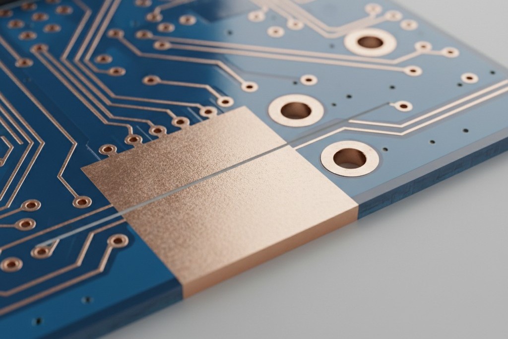
Relying solely on the chemical bond of the copper foil is a gamble professional engineers shouldn’t take. The adhesive layer between the copper and the dielectric is the weakest link in the stack-up. To prevent pad lifting, the design must introduce a mechanical lock—an anchor.
The most effective method utilizes the vertical structure of the PCB itself. A castellation pad shouldn’t just be top and bottom copper; it needs to be pinned together with dedicated vias. By placing one or two small vias (0.3mm is a standard mechanical drill size) near the inner edge of the pad—effectively “behind” the cut line—the top and bottom layers are riveted together through the core. Even if the router bit exerts enough force to delaminate the edge of the pad, the tear cannot propagate past these anchor vias. The copper is mechanically locked to the inner structure.
These anchor vias serve a dual purpose. During secondary reflow—when the module is soldered onto the mainboard—the heat stress on the edge pads is immense. Without anchors, the thermal expansion mismatch can cause the pads to float or peel, especially if hand-soldering rework is attempted. The anchor via acts as both heat sink and rivet. While some ultra-high-density designs might struggle to fit these anchors, omitting them invites field failure. If the pad lifts, there is no repair; the module is scrap.
Surface Finish as a Flatness Variable

The geometry of the cut is half the battle; the topography of the pad is the other. When a module is placed onto a carrier board, it must sit perfectly flat. Any deviation turns the module into a seesaw, leading to open joints on one side and crushed paste on the other.
Hot Air Solder Leveling (HASL) is fundamentally unsuited for castellated edges. The HASL process involves dipping the panel in molten solder and blowing it off with hot air knives. On a half-cut hole, this tends to leave a bulbous, uneven lump of solder at the edge. When the router comes through later to cut the board out, that lump of soft tin/lead (or lead-free alloy) smears and tears differently than the harder copper. More importantly, it creates a non-planar surface.
Electroless Nickel Immersion Gold (ENIG) is the mandatory standard for these applications. The nickel barrier layer provides a harder surface that cuts cleaner than soft solder, and the immersion gold ensures a perfectly flat, coplanar surface for the SMT process. While HASL is cheaper, the reject rate due to poor planarity and router smearing negates the savings instantly.
Communicating Intent: The Fab Note Firewall
The most common error in castellation design is silence. If the Gerber files contain a board outline running through a row of plated holes, but the fabrication notes say nothing, the CAM engineer at the factory has to guess. In a high-volume Tier 1 shop, automated scripts might flag it. In a quick-turn prototype shop, the operator might assume it’s a mistake or, worse, just run the standard profile routine.
A specific note on the fabrication layer is the only firewall against this. It must be explicit. A standard note might read: “Edge plating (castellations) present on J1 and J2. Vendor to use appropriate router entry/exit paths to prevent burring and copper lifting. IPC-6012 Class 3 acceptability criteria applies to edge plating conditions.” This forces the CAM engineer to acknowledge the feature, moving the liability from the designer’s omission to the manufacturer’s process.
The “Cheater’s” Castellation
There is a persistent myth, often circulated in hobbyist circles, that one can create castellations simply by placing a row of vias on the board outline and withholding that information from the fab house to avoid the surcharge. This is a “cheater’s” approach, and it is mechanically unsound.
When a standard router path cuts through a standard via without the special entry/exit considerations, the plating wall will almost certainly collapse or tear out. The structural integrity of a plated hole relies on it being a continuous cylinder. Once you slice that cylinder in half without precaution, the remaining half-cylinder loses its hoop strength. Without specific process steps to support that remaining wall, the “cheater’s” castellation results in a fragile, jagged edge that may not even take solder. It is a false economy.
Reliable hardware doesn’t hope the machine ignores physics; it survives by design. Anchor the pads, specify the finish, and write the note. The router bit doesn’t care about your deadline, but it will respect your geometry.
