The cost of a board respin goes far beyond scrapped panels and delayed timelines. For products mixing Quad Flat No-lead (QFN) and micro-Ball Grid Array (BGA) packages, the first-build yield cliff is steeper than most design teams anticipate. These two package families impose contradictory demands on nearly every aspect of manufacturing, from paste printing and component placement to post-reflow inspection. A stencil aperture optimized for a QFN’s large thermal pad will drown a micro-BGA’s fine-pitch balls in solder. A board rail sufficient for standard assembly may lack the rigidity needed when a heavy stencil spans both package types.
This conflict is rooted in the packages themselves. QFNs demand high paste volumes for a single large thermal pad—often 5mm or more on a side—while also requiring precise deposits on perimeter pads with pitches down to 0.4mm. Micro-BGAs, by contrast, distribute hundreds of solder balls across a small footprint at pitches of 0.5mm or finer, where even minor registration errors cause opens or bridges. When both share a common stencil and placement pass, the layout must reconcile these needs through deliberate, sometimes counterintuitive, DFM. Most avoidable first-build failures trace back to five specific decision points: paste aperture tuning, via-in-pad execution, underfill keepout planning, board rail dimensioning, and fiducial placement.
Why Mixed-Package Layouts Hit the First-Build Yield Cliff
The QFN’s exposed thermal pad is a notorious assembly challenge. This pad can represent 40 to 60 percent of the package footprint and requires a robust solder joint for thermal and electrical performance. This means sufficient solder volume is critical, yet the paste must reflow without trapping voids or causing the package to float. Surrounding this pad, fine-pitch perimeter leads demand precise paste deposits with minimal risk of slumping or bridging. The package is effectively two distinct assembly problems in one footprint.
Micro-BGAs impose a different set of constraints. With pre-attached solder balls, the variables shift from paste printing to placement accuracy. A 0.5mm pitch BGA allows only 0.1mm of error before balls miss their targets. The small pads, often just 0.25 to 0.3mm in diameter, require equally small and precise paste deposits. Too much paste causes bridging; too little leads to weak joints or opens. The margin for error is a narrow ±10 percent of the target volume.
When these packages coexist, a thick stencil that satisfies a QFN thermal pad will over-deposit paste on micro-BGA pads. A thin stencil optimized for the BGA will starve the QFN. The yield cliff appears when these conflicts are ignored. Solder joints on the QFN thermal pad show voids exceeding 25 percent, violating IPC-A-610 Class 3 criteria. Micro-BGA arrays exhibit bridging on inner rows or opens on corner balls. These are not random defects; they are deterministic failures rooted in predictable DFM mistakes.
Paste Aperture Tuning: Balancing Two Worlds
Solder paste volume, controlled by stencil aperture design, dictates joint quality. The volume must be enough to form a reliable joint and must release cleanly from the stencil. For mixed-package boards, hitting both targets demands careful tuning of aperture dimensions and stencil thickness.
Area ratio determines paste release. The ratio of the aperture area to its wall area must exceed 0.66 for reliable paste release. Below this, paste clings to the stencil walls instead of depositing cleanly. A 0.125mm thick stencil printing on a 0.25mm diameter micro-BGA pad yields an area ratio of roughly 0.5—well below the threshold. This forces a choice: reduce stencil thickness to improve the ratio for small pads, or accept larger apertures and risk over-depositing paste.
Stencil thickness is a necessary compromise. QFN thermal pads benefit from thicker stencils (0.150mm or more), while micro-BGAs perform better with thinner ones (0.100 to 0.125mm). When both share a stencil, the design must cater to the more constrained part. This usually means selecting a 0.125mm thickness and compensating for the QFN thermal pad by reducing its aperture area. While this means a smaller paste deposit on the thermal pad, it ensures acceptable BGA performance. Designs where QFN thermal performance is absolutely critical may require a costly dual-print process with two stencils.
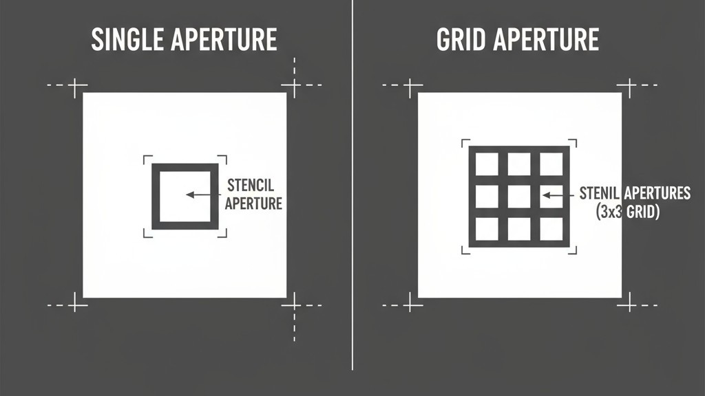
Thermal pad apertures need intentional reduction. A common guideline is to reduce the QFN thermal pad aperture area to 50-80 percent of the actual pad. This prevents the package from floating on excess solder during reflow and allows for a segmented aperture pattern. A grid of smaller openings, rather than one large window, improves paste release and reduces voiding by giving trapped flux an escape path. A typical 5mm thermal pad might use a 3×3 grid of 1.0mm square apertures, providing adequate solder volume while maintaining process control.
Our recommendation is to prioritize the micro-BGA. Select a thinner stencil for print resolution, then recover QFN thermal performance through via-in-pad design and careful aperture segmentation. This approach minimizes BGA bridging—the most difficult defect to rework—while accepting a manageable reduction in QFN thermal pad solder volume.
Via-in-Pad: Non-Negotiable Rules and Practical Limits
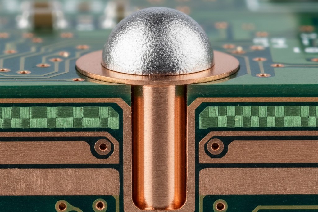
Vias inside component pads, common for QFN thermal management and micro-BGA escape routing, are a major reliability risk if not handled correctly. During reflow, the via barrel can wick solder away from the joint. At the same time, trapped air and flux can outgas, creating voids. Both mechanisms degrade the joint.
Copper-filled and planarized via processing is the most reliable solution. Here, the via barrel is plated with copper until completely filled, and the surface is ground flat. This eliminates the outgassing path and prevents solder wicking. The specification must be communicated clearly to the PCB fabricator, including a fill percentage of 95 percent or greater and the required surface finish. Reputable fabricators will certify this process to IPC-4761 or IPC-6012 Class 3 standards.
Non-conductive fill is a lower-cost alternative. An epoxy plug seals the via, blocking outgassing but not preventing solder wicking as effectively as a full copper fill. This approach may be acceptable for QFN thermal pads in less demanding Class 2 assemblies, but it is a weaker solution for micro-BGAs, where the paste volume budget is much tighter.
When Your Fabricator Can’t Guarantee Full Via Fill
If full via fill isn’t available or practical, the design must adapt.
- Via Tenting: Applying solder mask over the via opening provides a partial barrier. Tenting the top side of the board, directly under the pad, is most effective but relies heavily on solder mask registration accuracy.
- Plugging: Using non-conductive paste to plug the via is better than tenting but falls short of a full fill. The plug may not be planarized, leaving a surface depression that affects paste printing consistency—a significant risk for micro-BGAs.
- Accepting Open Vias: This is a last resort, viable only for prototypes or low-power QFNs where voiding up to 50 percent is tolerable. Open vias in micro-BGA pads are almost never acceptable due to the high risk of solder loss.
Treat filled via-in-pad as the baseline requirement for any production design mixing these packages. Explore alternatives only when fabricator constraints are absolute and the risks are explicitly documented.
Underfill Keepout Zones: Planning for Process Reality
Underfill, a liquid epoxy dispensed around a BGA, improves mechanical reliability by distributing stress across the solder joints. While not always required, it is common in applications subject to thermal cycling or shock. When specified, the board layout must accommodate the dispensing process.
The dispense needle requires a clearance of 1 to 2mm from the package edge for uniform flow. Components placed too close will obstruct the needle or create barriers, leading to voids and incomplete coverage. This keepout zone must be established early in the layout, as moving components later often forces a respin.
Component height within this zone is just as critical as lateral clearance. Tall components act as dams, blocking underfill flow. The layout should maintain a clear, flat area within the keepout, with no components exceeding the BGA’s standoff height (typically 0.3 to 0.5mm). For designs where rework is anticipated, this keepout should be extended to 3mm or more to allow access for removal tools.
Board Rails and Panel Design for Assembly
Board rails, the non-functional perimeter of a PCB panel, are the mechanical interface for all assembly equipment. Undersized or poorly designed rails cause the panel to warp during printing or shift during placement, crippling yield.
The minimum rail width for mixed QFN and micro-BGA assemblies should be 7 to 10mm per side. This provides enough grip area for conveyors and clamping mechanisms. Narrower rails, used to maximize boards per panel, invite flexure during stencil printing. The downward force from a heavy stencil can bow the panel, causing uneven paste deposits. The savings from narrower rails are almost always erased by yield loss. For boards thinner than 1.6mm, a temporary stiffener bar clamped to the rail during printing can prevent this flexure.
Tooling holes and fiducials on the rails provide reference points for automation. V-scoring or tab routing for depaneling also affects rail design. Mixed QFN and micro-BGA designs often benefit from tab routing, as it allows fine-pitch components to be placed closer to the board edge for better signal routing.
Fiducial Strategy: Accuracy Through Discipline
Fiducials, the optical reference marks for pick-and-place machines, directly determine placement accuracy. For these boards, where tolerances are measured in tens of microns, fiducial strategy is a primary design requirement, not an afterthought.
Global fiducials provide panel-level registration. Three non-collinear marks must be placed on the panel rails, as far apart as possible, to allow the vision system to calculate position, rotation, and scaling errors. Each global fiducial needs a clear keepout zone, typically a 3 to 5mm radius, free of any features that could confuse the vision system.
Local fiducials are required for each micro-BGA and are highly recommended for fine-pitch QFNs. They provide component-level registration, correcting for local board warpage. For a micro-BGA, two local fiducials placed diagonally across the package, within 10 to 15mm of its edge, provide optimal accuracy.
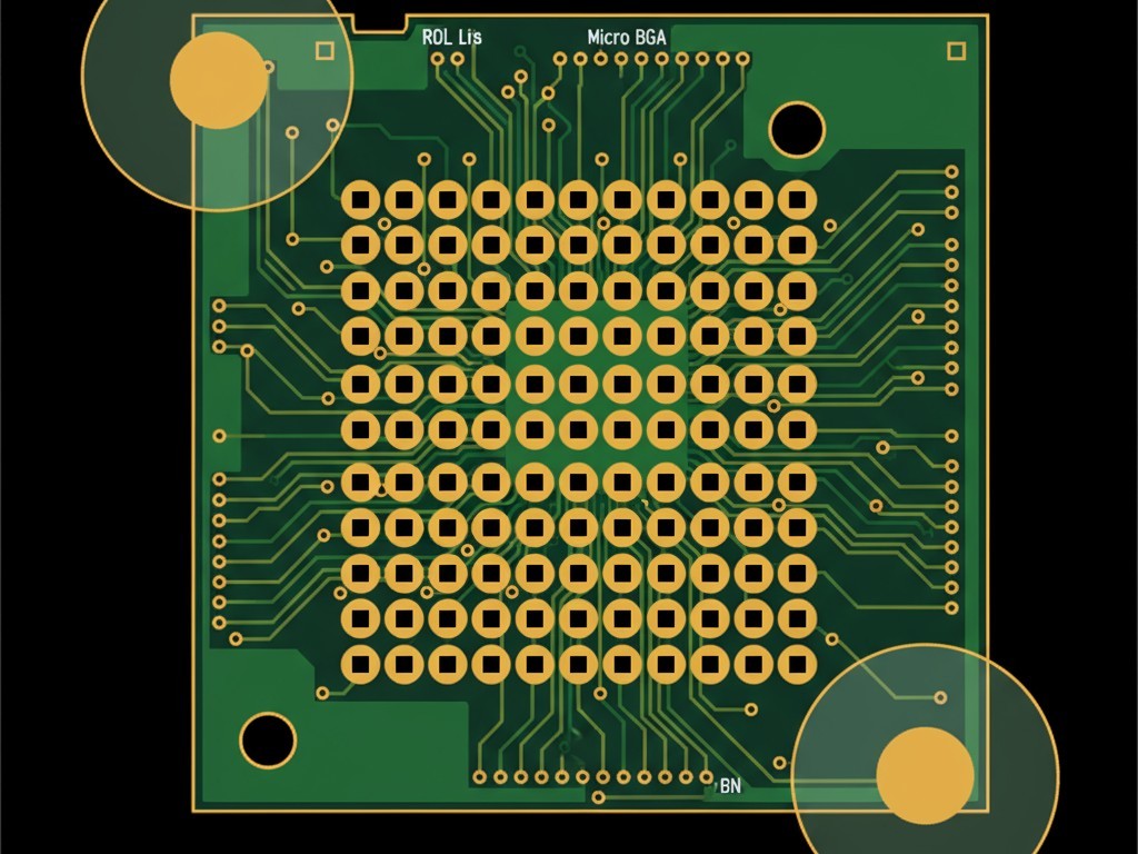
A typical fiducial is a 1mm diameter bare copper circle inside a 2mm circular solder mask opening. This ensures high contrast for the vision camera. In dense layouts where ideal spacing isn’t possible, the distance can be reduced to a 5mm minimum. As a last resort, a large QFN corner pad or BGA corner ball pad can be designated as a fiducial target, but this is a high-risk strategy.
The Final Gate: Pre-Tape-Out DFM Verification
A systematic review of these five critical areas before tape-out is the final chance to catch errors.
Verification should begin with a peer review focused on these specific high-risk areas. Automated DFM software can flag some issues, but it cannot evaluate the nuanced trade-offs in paste aperture design or via-in-pad choices. Human judgment is essential. Follow this with a consultation with your intended fabricator and assembly house. Sharing your data allows them to identify process-specific risks before the design is locked.
Your pre-tape-out checklist must include:
- Stencil Apertures: Data exported and reviewed for correct area ratios on all micro-BGA pads and proper reduction on QFN thermal pads.
- Via-in-Pad: Specifications clearly documented in fab notes, including fill method and acceptance criteria.
- Underfill Keepouts: Zones verified for all micro-BGAs, with no components violating clearance.
- Board Rails: Width confirmed to meet minimum dimensions for panel stiffness.
- Fiducials: Global and local placement verified for size, spacing, and keepouts.
- Solder Mask: Clearances on micro-BGA pads confirmed to be non-solder mask defined (NSMD).
- Depaneling: Method and edge clearances verified to prevent component damage.
Completing this gate transforms DFM from an abstract goal into a measurable outcome. It is the difference between a smooth first build and a costly respin.

