Field returns often trace back to the same quiet failure: voids beneath the thermal pad of a QFN package. The product passed initial testing, shipped to customers, and then began failing under sustained thermal load. For engineering managers reviewing root cause analyses, the diagnosis is frustratingly consistent. Incomplete solder wetting on the large copper thermal pad created voids that degraded heat transfer, leading to premature component failure. The reflex is to tweak reflow profiles or adjust stencil apertures, but these are merely bandages on a deeper wound.
The variable most teams overlook is the surface finish. Where HASL creates the conditions for thermal pad voiding, ENIG quietly prevents them from forming in the first place. The difference isn’t abstract plating chemistry but a tangible mechanical reality: the planarity of the finished surface determines whether solder can wet completely and flux can escape during reflow. On the fine-pitch, high-thermal boards where QFNs are common, this distinction becomes the line between reliable production and costly field failures.
Understanding this distinction is key. The argument for ENIG isn’t about chasing perfection; it’s about managing risk. It’s about weighing a minor increase in board cost against the major, unrecoverable costs of thermal instability, stencil design compromises, and failures in the field.
Why QFN Thermal Pads Develop Voids
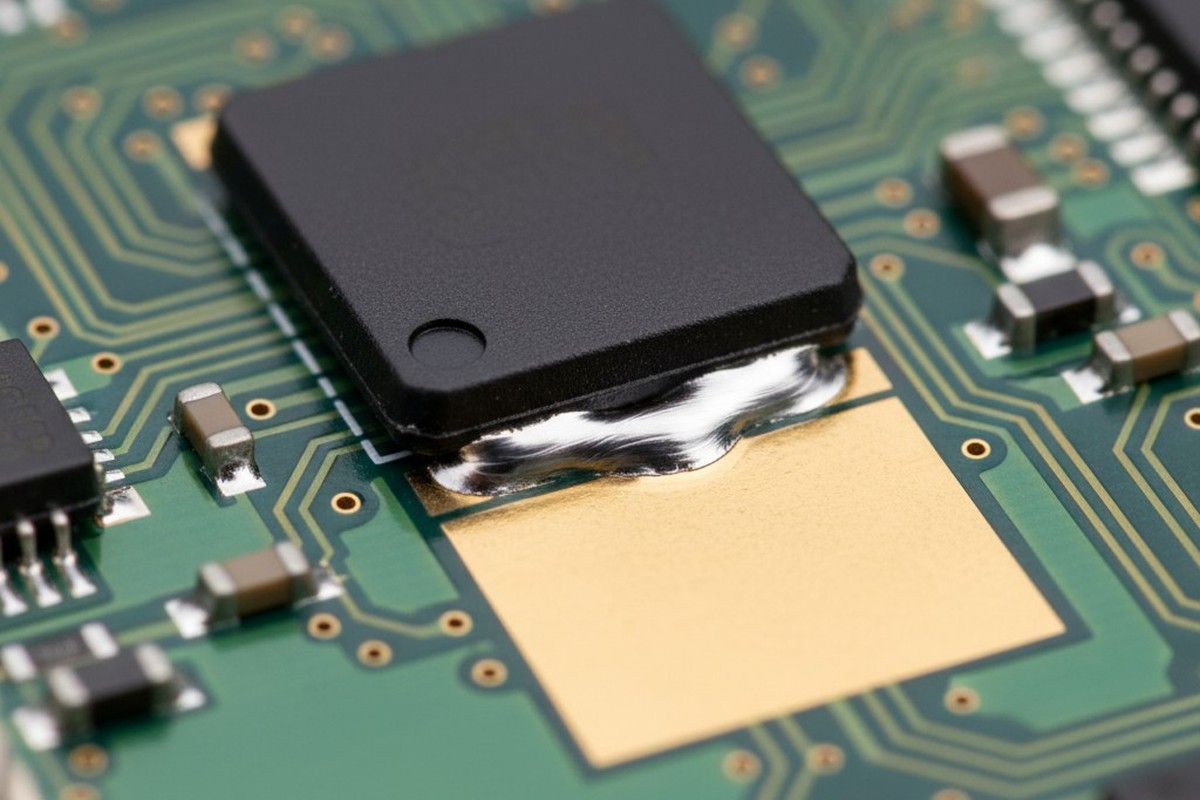
QFN packages use a large central thermal pad to dissipate heat efficiently into the PCB. This pad, often several millimeters square, is fundamentally different from the small perimeter signal pads. It is a single, continuous copper area engineered to create a low-resistance thermal pathway from the die to the board. While essential for thermal performance, its size and continuity create a challenging environment for solder paste during assembly.
During reflow, the solder paste on this pad transforms. The paste—a mixture of solder spheres suspended in flux—heats, and the flux activates to clean the metal surfaces before it volatilizes. The solder spheres then collapse into a molten pool. For small signal pads, this process is simple. The paste volume is small, the molten solder quickly wets the copper, and the vaporized flux escapes easily from the pad’s edges.
The thermal pad is another story. Its large area requires more paste, which means more flux and a much longer path for outgassing. As the solder collapses, it tries to wet the entire pad surface at once. If the surface topology is uneven or the solder wets non-uniformly, pockets of flux become trapped beneath the solidifying metal. These trapped pockets are voids, and they are not cosmetic defects. Each one reduces the effective contact area between the QFN and the PCB, creating localized hotspots of high thermal resistance. Under sustained operation, these hotspots accelerate component degradation, leading directly to the field failures engineering teams are paid to prevent.

Void formation isn’t random. It is a direct consequence of how solder wets a surface and how flux escapes during the brief window of reflow—both of which are controlled by the surface finish.
The Surface Finish Divide: Planarity as the Hidden Variable
The critical difference between ENIG and HASL is not a subtle materials science nuance; it is a matter of surface geometry. HASL produces a surface that is scalloped, uneven, and highly variable in thickness. ENIG produces a surface that is conformal, uniform, and flat to within sub-micron tolerances. This planarity is the root cause of ENIG’s superior performance on QFN thermal pads.

HASL (Hot Air Solder Leveling) is applied by dipping a PCB into molten solder and blasting the excess off with hot air knives. The result is a coating that follows the underlying copper but with significant topographic variation. Thickness can range from 1 to 40 microns, and the surface has a characteristic wavy texture from the air leveling. On small pads, this unevenness is often inconsequential. On a large thermal pad, the scalloped topology creates a landscape of peaks and valleys where molten solder struggles to penetrate and flux gases have no clear escape route. The surface itself acts as a barrier, trapping flux in low-lying areas as the solder solidifies on the high points. These trapped regions become voids.
ENIG (Electroless Nickel Immersion Gold) is a plating process. A thin layer of nickel is chemically deposited onto the copper, followed by a protective flash of gold. The process is inherently conformal, tracing the copper surface with near-perfect fidelity while adding only 3 to 5 microns of nickel and a fraction of a micron of gold. The resulting surface is not just smooth; it is predictably flat. There are no scallops, no thickness gradients, and no topographic barriers to solder flow.
This flatness has a direct mechanical consequence. During reflow, molten solder on a flat ENIG surface wets radially and uniformly. The flux, being less dense, is pushed outward toward the pad edges where it can volatilize freely. The solder collapses into full contact with the nickel, leaving no pockets where flux can be trapped. The same solder paste on a HASL surface encounters a complex landscape where flux gets trapped in the valleys before it can escape. The difference is measurable: ENIG thermal pads routinely exhibit void percentages below 5%, while HASL pads on the same assembly often exceed 20% to 30%.
How HASL’s Thickness Variability Compounds Voiding
Fine-pitch layouts make HASL’s unevenness even more problematic. When signal pads are closely spaced, the risk of solder bridging increases. To mitigate this, engineers often reduce stencil thickness or shrink aperture sizes to deposit less paste. This is a manageable trade-off for small signal pads, but it starves the thermal pad if the same stencil is used across the board.
A thinner paste deposit on HASL’s already uneven surface exacerbates incomplete wetting. There is simply less molten solder available to flow into the valleys of the scalloped topology, increasing the probability of flux entrapment. The result is higher voiding rates on fine-pitch boards with HASL—precisely the boards where thermal performance is most critical. ENIG’s flat surface eliminates this compounding effect. Its uniform topology allows complete wetting even with reduced paste volumes, making stencil design less of a balancing act.
Heat Transfer Stability and Long-Term Reliability
A thermal pad’s sole purpose is to move heat from the QFN die to the PCB, where it can be dissipated through copper planes or heat sinks. The efficiency of this transfer depends on the thermal conductivity of the solder joint and the completeness of the physical contact. Voids degrade both.
Each void is an island of zero thermal conductivity. Heat must flow around it, creating a localized increase in thermal resistance. A single large void or a cluster of smaller ones can raise a component’s junction temperature by several degrees Celsius under load. For high-power devices or components operating near their thermal limits, this increase is the difference between reliable operation and accelerated wear. A component may pass initial functional tests, but sustained thermal cycling in the field will lead to solder fatigue, intermetallic growth, or outright thermal runaway.
ENIG’s low-voiding performance delivers a stable, predictable thermal resistance over the product’s life. The uniform nickel-solder interface formed during reflow is robust, and the planarity that prevented voids during assembly ensures full contact during thermal cycling. By contrast, HASL joints often start with compromised thermal contact and can degrade further as the scalloped interface promotes non-uniform intermetallic growth. For boards with strict thermal requirements—like LED drivers, power converters, or RF amplifiers—the surface finish isn’t incidental. It determines whether the thermal design will perform as modeled.
Stencil Windowing Strategies for ENIG
ENIG’s planarity opens up opportunities to optimize stencil design specifically for thermal performance. The flat surface allows solder paste to release cleanly from apertures, enabling aggressive windowing patterns that would be unreliable on HASL.
The key parameter is the area ratio, defined as the aperture opening area divided by the aperture wall area; a ratio of 0.5 to 0.6 is a common minimum for good paste release. ENIG’s smooth surface reduces friction during stencil separation, making it possible to use even lower area ratios if needed. More importantly, it enables “windowpane” patterns—dividing the large thermal pad aperture into a grid of smaller openings—without the release failures that would plague a rough HASL surface.
Windowed stencils offer two clear benefits. First, they improve paste release consistency by increasing the perimeter-to-area ratio of each opening. Second, they create multiple distinct solder deposits that coalesce during reflow, giving flux more channels to escape than a single large deposit would allow. A common strategy for a 5mm thermal pad is a 3×3 or 4×4 grid of square apertures covering 80% to 90% of the total pad area. The gaps between the squares become vents for flux during the critical collapse phase of reflow.
This strategy hinges on ENIG’s flatness. On HASL, the scalloped surface would cause inconsistent paste release across the windowpanes, leading to uneven solder deposits and, paradoxically, more voids. ENIG allows the stencil to be a tool for mitigating voids rather than a source of variability.
While other flat finishes like OSP or Immersion Silver offer similar stencil release benefits, they lack ENIG’s robustness. OSP can oxidize if boards are not assembled promptly, and Immersion Silver can tarnish or suffer from multiple reflow cycles. ENIG’s gold layer provides a stable, solderable surface that tolerates handling, delays, and rework.
The Real Cost of Switching
Cost is the most common objection to ENIG, and it deserves a precise answer. While ENIG is more expensive than HASL per board, the delta is smaller and more context-dependent than many assume. For small to mid-volume production (runs of 100 to 5,000 boards), the incremental cost is measurable in cents or dollars per board, not abstract percentages.
Typically, ENIG adds $1.50 to $3.00 per square foot of board area compared to HASL. For a 100mm x 100mm board, this translates to roughly $0.20 to $0.40 per board. On a 500-board run, the total difference is $100 to $200. On a 5,000-board run, it’s $1,000 to $2,000. These are real costs, but they are finite and predictable.
The cost of a single field return, however, is not. RMA processing, failure analysis, replacement units, and reputational damage can easily run into thousands of dollars per incident, dwarfing the total ENIG upcharge for an entire production run. If ENIG eliminates even one field failure caused by thermal pad voiding, the investment pays for itself. For products with high-power components or those deployed in demanding environments, the probability of a voiding-related failure on HASL is not negligible. ENIG drives that probability toward zero.
For low-power applications where a QFN operates well below its thermal limits, or for non-critical products where occasional failures are tolerable, HASL may be an acceptable choice. The voiding will still occur, but if the thermal margin is large enough, the component will function despite it. This is a risk calculation, not a technical equivalence. ENIG eliminates the risk; HASL requires the margin to absorb it.
Making the Case to Leadership
The argument for ENIG is not about it being a “premium” finish. The argument is that it solves a specific, predictable failure mode that HASL cannot. The causal chain is direct: HASL’s scalloped topology traps flux, creating voids under QFN thermal pads. Those voids degrade heat transfer, increasing junction temperatures and causing component failures in the field. ENIG’s conformal planarity allows flux to escape and solder to wet completely, eliminating the voids and ensuring thermal stability.
When presenting this to leadership, the frame is risk mitigation. The modest cost of ENIG is an investment to avoid the much larger, unpredictable cost of field returns, warranty claims, and redesigns. The mechanism is proven, the cost delta is small, and the alternative is to accept a known defect mechanism and hope that your thermal margin is wide enough to absorb it.
On the fine-pitch, high-thermal boards where QFNs are essential, hope is not a reliable engineering strategy.
 Circuit Board Assembly")


