The silence of a dead prototype is heavy. It isn’t just the lack of fan noise or the dark LEDs on the debug interface. It’s the immediate, sinking calculation of cost. When a prototype board fails to initialize—maybe a BGA didn’t seat correctly during assembly, or a design flaw demands a swap—focus instantly narrows to the large, black square in the center of the PCB.

In high-reliability sectors, that square is often a high-end FPGA, like a Xilinx Kintex UltraScale or an Intel Stratix 10. These aren’t commodity components; they are assets. In times of supply chain constriction, replacing that single chip might involve a 52-week lead time or a broker market markup that breaks the project budget. The board itself, a 12-layer stack-up with blind and buried vias, might represent $5,000 in fabrication and assembly costs. Rework isn’t standard repair. It’s a salvage operation where the entire development timeline is at stake.
Physics Doesn’t Negotiate
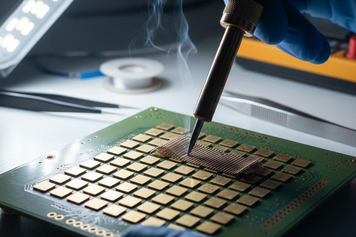
A dangerous misconception persists that removing a Ball Grid Array (BGA) is simply a matter of applying heat until the solder melts. This attitude destroys prototypes. Handheld heat guns, while great for shrinking tubing, are instruments of destruction for high-density interconnects.

The physics comes down to thermal mass and the coefficient of thermal expansion (CTE). A modern FPGA sits on a board filled with copper ground planes designed specifically to dissipate heat. If you blast the top of the chip with hot air without adequately heating the bottom of the board, you create a vertical thermal gradient. The top expands while the bottom remains cool and rigid. The result is warping. As the board bows, it pulls against the solder joints. If the heat source is uncontrolled, you risk “pad cratering”—literally ripping the copper pads out of the fiberglass laminate. Once a pad is torn from an internal trace, the board is scrap. No amount of jumper wire can reliably fix a high-speed differential pair running at 10 Gbps.
This is why engineers must adopt a “localized manufacturing” mindset. The goal is to replicate the original reflow profile—the specific curve of temperature over time—that the board saw in the manufacturing oven. The entire assembly must be brought up to a soak temperature (usually around 150°C to 170°C) to activate the flux and equalize the temperature across the PCB. Only then should you apply localized energy to the component itself to push it past the liquidus point of 217°C. Physics ignores deadlines; if the thermal ramp is too steep, moisture trapped inside the chip package expands into steam, causing the package to delaminate or “popcorn.” A popped chip is a dead chip.
The Process: Controlled Intervention
Saving a $2,000 component demands rigor. The process begins days before the actual rework with moisture management. Unless the board has been stored in a dry box with humidity indicators reading safe levels, it must be baked. Standard IPC-1601 protocols dictate baking the moisture out of the PCB and the component to prevent that steam-pressure delamination. Skipping this step is the most common cause of invisible failures appearing weeks later.
Once the board is dry, it moves to a dedicated rework system—typically a machine with split-vision optics, bottom-side infrared preheaters, and a computer-controlled top convection nozzle. Automation drives this process, not manual feel. A thermocouple is often attached to a sacrificial board to map the thermal profile exactly. We need to know that when the machine says 230°C, the solder balls underneath the center of that 35x35mm grid are actually reaching reflow, not sitting cold due to a nearby heat sink.
The removal itself is anti-climactic if the profile is correct. The vacuum nozzle descends, the solder liquefies, and the component lifts vertically with zero force. The anxiety peaks immediately after: site dressing. This involves manually removing old solder from the PCB pads using a soldering iron and wicking braid. This is where the hands of the technician matter most. The iron must “float” over the pads; any downward pressure risks lifting a pad, which is usually fatal to the board. While epoxy repair methods exist for lifted pads, the impedance mismatch introduced by a repair is often unacceptable for high-frequency FPGA lines. The pads must be pristine, flat, and copper-bright before a new or reballed chip can be placed.
The Reballing Equation

Sometimes the goal isn’t a new chip, but salvaging the old one from a dead board to use elsewhere, or re-seating a chip that had a connection failure. This introduces the sub-discipline of reballing. A removed BGA has messy, irregular bumps of solder left on its underside. These must be wicked off and new solder spheres attached.
It’s a pure ROI calculation. Reballing a $5 commodity microcontroller is financial nonsense; the labor hours exceed the component cost. But for a Virtex UltraScale+ worth $15,000, reballing is mandatory. The process involves a specific stencil matching the chip’s footprint, a tacky flux, and thousands of pre-formed solder spheres (often 0.4mm or 0.5mm in diameter) manually poured and aligned.
Uncertainty is unavoidable, though. Every time a silicon die undergoes a reflow cycle—heating to 240°C and cooling down—thermal stress accumulates. The mismatch in thermal expansion between the silicon die, the package substrate, and the PCB exerts force on the internal interconnects. While a chip can usually withstand two or three reflow cycles (initial assembly, removal, reballing, placement), yield is never guaranteed. We can mitigate risk with perfect profiling, but we cannot change the fatigue limit of the materials.
The decision to rework usually comes down to the “replace vs. recover” ratio. If the silicon is irreplaceable due to shortages, or if the board represents weeks of unique fabrication time, the investment in a proper thermal profile and skilled operator time is negligible compared to the cost of starting over. The equipment—the pre-heaters, the vision systems, the nitrogen-inerted reflow heads—exists to turn a catastrophe into a standard engineering delay.


 PCB Technology: Types, Benefits, Challenges, and Applications")

