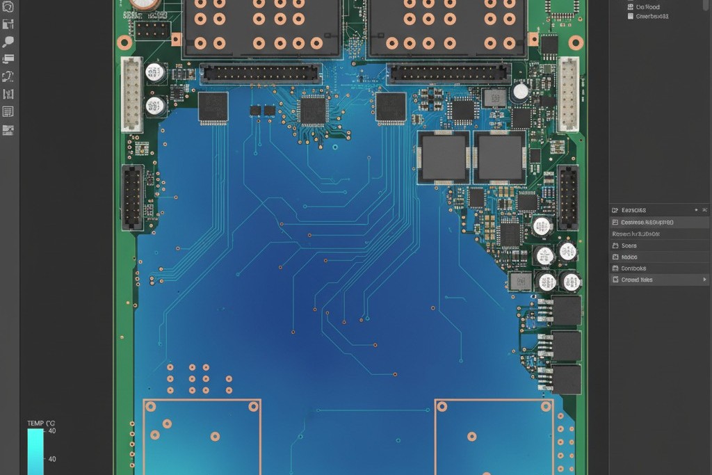
You spend weeks on the layout. The schematic is verified, the DRCs in Altium are clean, and the power planes are massive slabs of 3oz copper designed to carry 100 amps without breaking a sweat. On screen, it looks like a masterpiece of low-impedance routing. The nets are fully connected, the airwires are gone, and the simulation shows a beautiful, cool blue path for your current.
Then the boards come back from the fab, and they’re bricks.
Connectors snap off because the solder joints are cold and granular. Power FETs fail in the field because they never actually wetted to the pad, creating a high-resistance contact that heats up and eventually cracks. You haven’t designed a circuit. You’ve designed a heat sink that swallowed the thermal energy of the reflow oven whole.
This is the fundamental conflict of power PCB design. The copper geometry required to move massive current is often the exact same geometry that prevents a reliable solder joint. Physics doesn’t care about your netlist connectivity. If you can’t get the solder to flow, you don’t have a board.
The Thermodynamics of a Brick
Stop thinking like an electrical engineer and start thinking like a plumber dealing with heat flow. When you place a component pad directly onto a large copper plane (especially one that is 2oz, 3oz, or heavier), you are connecting a small pool of molten metal to a massive thermal reservoir.
When the reflow oven or soldering iron touches that pad, it tries to raise the local temperature to the melting point of the solder—typically around 217°C for SAC305. However, copper is an exceptional conductor. That massive ground plane acts as a highway, wicking thermal energy away from the pad faster than the heat source can supply it. It’s like trying to fill a bucket with a fire hose draining out the bottom. You can turn your soldering iron up to 450°C and risk damaging the adhesive holding the copper to the FR-4, but it won’t matter. The heat isn’t staying at the joint; it’s dissipating into the plane.
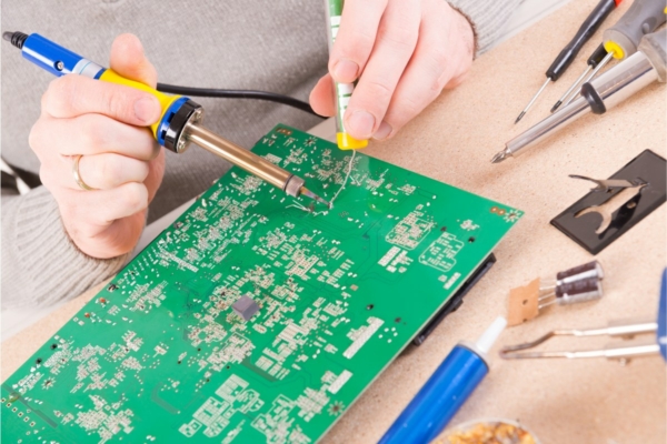
The result is a “cold joint.” The solder might melt on the component lead, but it freezes the moment it touches the copper pad. It balls up, sitting on the surface like a bead of mercury rather than flowing out into a smooth fillet. If a technician tries to force it by holding the iron there for 45 seconds, they usually just delaminate the pad or burn the flux away before wetting occurs. This is usually where people blame their tools, thinking they need a higher wattage iron. But even a Metcal MX-500 with a heavy hoof tip can’t fight a 4oz plane without help. Thermal mass wins every time.
The “Direct Connect” Myth
A persistent myth in power electronics claims that high-current paths must use direct connect polygons. The logic seems sound: any restriction in the copper path increases resistance, which increases heat. Therefore, to minimize heat, we must maximize copper contact.
That logic is dangerous because it ignores the manufacturing floor. A direct connection that results in a cold solder joint will have significantly higher contact resistance than a properly wetted joint connected via thermal relief spokes. That cold joint is a ticking time bomb. Under thermal cycling—like a motor controller heating up and cooling down—the granular structure of the cold solder cracks. Once it cracks, resistance skyrockets, the joint heats up, and you eventually get a catastrophic open circuit or a fire.
This isn’t limited to big connectors, either. The same thermal imbalance causes tombstoning on smaller passives. If you have a 0603 capacitor connecting a signal trace to a ground plane and you use a direct connect on the ground side, the solder on the signal side melts first. Surface tension pulls the component upright, standing it on end. The reflow oven heats the board evenly, but the board doesn’t accept the heat evenly. Unless you are doing RF work where impedance discontinuities are critical, or dealing with pulse currents so high they would vaporize a spoke instantly, direct connect on power planes is usually a design defect masquerading as an optimization.
Calculating the Compromise
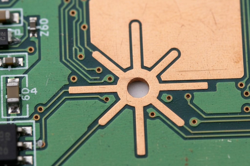
Enter the thermal relief: those wagon-wheel spokes connecting the pad to the plane. They act as a thermal dam, restricting the flow of heat just enough to allow the pad to reach temperature during the 60-90 seconds of the reflow window.
Here is where the fear sets in. If you make the spokes too thin, they become fuses.
CAD defaults will kill you here. Standard rules in KiCad or Eagle are often tuned for signal layers, creating 10-mil spokes that vaporize the instant you push 20 amps through them. You have to calculate the spoke width based on the actual load. It’s a trade-off: enough copper to carry the current, but little enough to block the heat.
Start with the basics. Determine the current per pin. If a connector pin carries 40 amps, don’t assume the spokes need to carry 40 amps alone. Usually the pin itself is the bottleneck, but let’s say you need to support that load. Use the IPC-2152 standard to determine the trace width required for a given temperature rise. If you need 100 mils of copper width to carry that current with a 10°C rise and you have four spokes, each spoke needs to be 25 mils wide.
But wait. A 25-mil spoke on 3oz copper is still a significant heat pipe. It might be too thermally conductive for a standard reflow profile. You might need to reduce the spoke count to two wider spokes, or increase the spoke length to create a longer thermal path. It’s an iterative process. You are balancing the risk of the spoke fusing (electrical failure) against the risk of the joint never wetting (mechanical failure).
There is uncertainty here. IPC standards are conservative, and real-world performance depends on airflow and the thermal conductivity of your specific substrate. But you are better off trusting the math of the Saturn PCB Toolkit than guessing. And while some designers try to cheat by stitching vias around the pad to increase vertical current flow, remember that every plated through-hole is another thermal anchor dragging heat away from the surface.
DFM Reality: The Technician’s Struggle
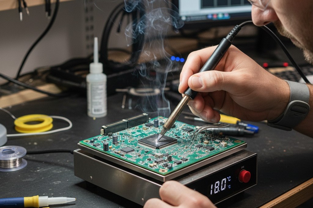
Ignore these calculations and flood the plane, and you effectively declare war on the assembly floor. When a board with poor thermal relief hits the rework bench, it becomes a nightmare.
Picture a technician trying to replace a MOSFET on your board. They apply the iron. Nothing happens. The solder doesn’t melt. They add fresh solder to the tip to increase the contact area. Now it’s a slushy mess. They have to grab the hot plate, strap your board down, and pre-heat the entire assembly to 150°C—baking the electrolytes in your capacitors—just to lower the thermal delta enough that the iron can bridge the gap.
This thermal stress degrades the FR-4 material and shortens the life of every other component on the board. You might save 2 milliohms of resistance by using a direct connect, but you cost the company thousands in rework time and scrapped assemblies. A board that cannot be reworked is a disposable board. Unless you are building throw-away consumer toys, reworkability is a hard requirement.
Design for the Oven
The goal is simple: trick the heat into staying where you need it, just long enough to form the intermetallic bond that makes a solder joint real.
Don’t let the CAD tool push you around. Go into the design rules. Set up specific classes for your power nets. Force the software to use calculated thermal spokes rather than global defaults. It takes an extra hour during the layout phase to set up these rules and verify them. That hour saves weeks of spin time when the first prototype run comes back with connectors falling off the board.
We often get lost chasing the perfect electrical schematic, assuming that if the electrons have a path, the job is done. But the electrons never get a chance to flow if the manufacturing process fails. Heavy copper requires heavy thinking about thermodynamics. Respect the heat, choke the flow at the pad, and let the solder do its job.

