What is Component Kitting
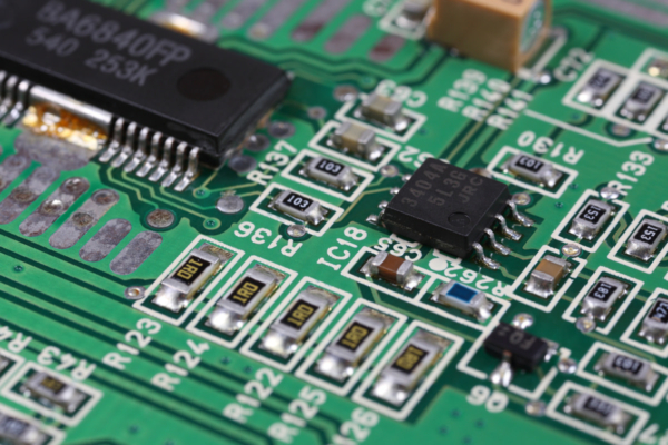
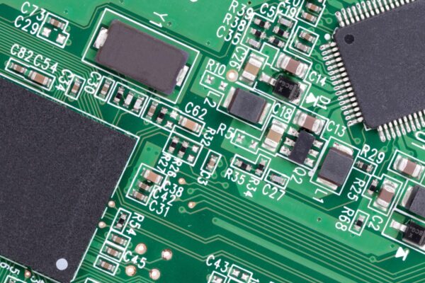
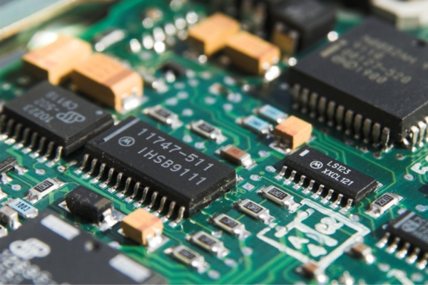
Component kitting is the process of gathering and organizing all the necessary electronic components required for the production of a PCB assembly. It involves preassembling these components into kits or packages that contain all the parts needed to complete a device. The purpose of component kitting is to streamline the manufacturing process by ensuring that all the required components are readily available, properly labeled, and organized.
By utilizing component kitting, companies can improve efficiency, reduce assembly time, and minimize the risk of errors or missing parts during production. The kits are typically delivered to the point of assembly when they are needed, eliminating the need for daily sorting and compiling of parts. This not only saves time but also reduces the risk of mistakes or component shortages.
In addition to improving production efficiency, component kitting offers other benefits. It helps to optimize workspace by reducing clutter and crowded work areas. It also contributes to a reliable supply chain by ensuring that the necessary components are readily available and can be easily sourced. This reduces the risk of delays or disruptions in production.
Frequently Asked Questions
What Are the 3 Main Phases in Creating a PCB
PCB Development involves three main phases that are crucial for taking a circuit board design from conception to production. These phases are commonly known as design, manufacturing, and testing.
What Is 7 Layer PCB
A 7 layer PCB is a type of multilayer board that is considered more advanced. It is composed of seven copper layers, including power planes, ground planes, and routing layers. Due to the additional routing layers, a 7 layer PCB is well-suited for high-speed applications.
How Many Types of PCB Design Are There
There are several types of PCB designs available, including Single Sided PCB or Single Layer PCB, Double Sided PCB or Double Layer PCB, Multilayer PCB, and Rigid PCB.
How Thick Is 12 Layer PCB
The typical thickness of a 12-layer PCB is 1.6mm.
How Thick Is 16 Layer PCB
The 16 layer PCB is made of FR4 material with a TG170 (ITE180) rating. Its thickness measures 2.0mm, and each panel measures 200*300 mm with 6 units per panel.
Can a PCB Have Multiple Layers
Multilayer PCBs are composed of three or more layers of conductive material within the insulating material, making them distinct from double-sided PCBs that only have two layers of conductive material on the top and bottom. Therefore, a PCB can have multiple layers if it has more than two layers of conductive material.
Can You Put Components on Both Sides of a PCB
Similar to other surface mount components, it is possible to mount them on both sides of a printed circuit board for a reflow soldering process, making it a double-sided PCB.
What Is Type 4 PCB
2 Type 4 (also known as HDI) PCBs are classified as PCBs that employ blind, buried, or microvia technologies. A blind via is drilled starting from the surface layer and ends on an internal layer, whereas a buried via is only drilled on internal layers and is not present on the surface layers.
What Is the Most Common PCB
Most commercial PCB mixtures in the United States are commonly referred to by their industrial trade names, with the most prevalent one being Arochlor.
What Are the 4 Stages of PCB Design Flow
We can divide the prototyping stage shown above (Design > Prototype > Validate) into four stages: Part Research and Selection, Schematic Capture and Simulation, Board Layout, and Verification and Validation.
How Many Layers Does a PCB Have
PCBs with four layers are printed circuit boards that consist of four conductive layers: the top layer, two inner layers, and the bottom layer. The inner layers, known as the core, are typically utilized as power or ground planes, while the top and bottom outer layers are designated for component placement and signal routing.
How Far Should Components Be From Edge of PCB
Board Edge Clearance for PCB Components and Connectors
It is recommended to maintain a minimum distance of 0.04” between all components and connectors from the board edge. Additionally, resistors and capacitors should be placed even further away from the edge.
What Is the Rule for PCB Spacing
Under the IPC 2221 voltage and spacing standards, the minimum requirement for PCB spacing (specifically, the clearance between any two conductors) is 0.1 mm for general-purpose devices or 4 mils. However, for power conversion devices, the minimum PCB trace width and spacing should be 0.13 mm or 5.1 mils.
What Is PCB Layout vs Design
A PCB schematic is a basic circuit design that visually represents the functionality and connectivity of different components in a two-dimensional format. In contrast, PCB designs are three-dimensional layouts that illustrate the specific locations of these components once the circuit’s functionality has been confirmed.
Why Capacitor Is Used in PCB
Capacitors are utilized in PCBs to maintain a consistent voltage level. These electronic components effectively reduce voltage fluctuations. When the voltage is present in the parallel circuit, the capacitor becomes charged. Additionally, the current discharged from a capacitor is in the form of alternating current.
What Is PCB Life Cycle
The PCB life cycle encompasses two main stages: board fabrication and PCB manufacturing.
What Are Four Types of Assembly
Assembly language consists of four types: RISC (Reduced Instruction-Set Computer), DSP (Digital Signal Processor), and CISC (Complex Instruction Set Computer).
What Are the 4 Parts of Assembly
It consists of four components: label, mnemonic, operand, comment. However, not all of these parts are present in every line. The label, which is a word created by the programmer, serves as an identifier for a specific point in the program.
What Is RTL vs Netlist
The term “RTL” refers to the functionality of a device that is written in a language like Verilog or VHDL. It represents the behavior of the device at a higher level of abstraction. On the other hand, a netlist is a gate-level description of the device that is obtained after synthesizing the RTL. So, in summary, RTL is the higher-level representation of the device’s functionality, while the netlist is the gate-level description.
What Is the Difference Between Schematic and Netlist
In comparison to schematics, netlists offer a straightforward data format for describing all connections in a PCB design through text. They encompass reference designators, pin numbers, and signal keywords.
