The wireless range on your IoT product’s datasheet is a promise made in a controlled lab. That promise breaks quietly on the production floor when assembly alters the electromagnetic behavior of your antenna. A board that achieved –2 dB return loss and 85% radiated efficiency in prototype can easily degrade to –6 dB and 60% efficiency after volume assembly. The failure is invisible until a device is in the field.
At Bester PCBA, preserving RF performance through assembly isn’t an aspiration; it’s an engineered outcome. We enforce four distinct manufacturing disciplines: antenna keepout zone compliance, controlled impedance stackup preservation, low-residue flux processes in RF-critical areas, and test jig design that validates radiated performance without introducing new variables. These controls are not just safeguards. They are an interdependent system, and a failure in one discipline compromises the others.
The core problem is detuning. An antenna is a resonant structure whose performance depends on a precise electrical length and impedance match to its transmission line. Assembly introduces variables like material contamination, dielectric shifts, and ground plane disruption that alter these properties. While the changes may be small in absolute terms, they are catastrophic to RF performance. A mere 5% shift in the effective dielectric constant near a 2.4 GHz antenna can move its resonance by 120 MHz, turning a well-matched radiator into a poorly matched load that reflects power instead of transmitting it.
Why Antennas Detune During PCB Assembly

An antenna resonates when its physical geometry corresponds to a fraction of its target electromagnetic wavelength. A quarter-wave monopole antenna for 2.4 GHz is about 31 millimeters long in free space, but an antenna never operates in free space. It exists in the electromagnetic environment of the PCB substrate, its ground plane, and any nearby materials. The antenna’s effective electrical length is determined by both its physical dimensions and the dielectric constant of its surroundings. When assembly alters that environment, the antenna detunes.
Three primary mechanisms cause this detuning, each operating through a distinct physical pathway. Understanding them is the foundation for manufacturing controls that address root causes, not just symptoms.
Material contamination alters dielectric loss. Flux residues, solder paste particles, and cleaning agents left near the antenna introduce lossy dielectric materials into its near-field region. These contaminants increase the loss tangent of the surrounding medium, causing more electromagnetic energy to dissipate as heat instead of radiating into the far field. In practical terms, a contamination layer with a loss tangent of 0.02 can reduce a patch antenna’s radiated efficiency from 80% to 65%—a loss of nearly 1 dB in effective radiated power.
Dielectric constant shifts change the effective wavelength. A PCB substrate’s dielectric constant isn’t fixed; it varies with temperature, humidity, and absorbed moisture. During reflow soldering, the substrate can reach 250°C. If an antenna was tuned at room temperature on a substrate with a dielectric constant of 4.4, and reflow-induced changes push that value to 4.6, the resonant frequency shifts downward. For a 2.4 GHz antenna, this 4.5% increase corresponds to a frequency shift of about 100 MHz. The antenna is now resonant at 2.3 GHz, and its performance at the intended 2.4 GHz operating frequency degrades significantly.
Ground plane disruption changes impedance matching. An antenna’s ground plane is not passive; it is an active part of the radiating system, acting as a counterpoise or reflecting element. Its size, shape, and continuity directly affect the antenna’s input impedance. Assembly processes that introduce mechanical stress from depanelization or fixturing can deform the ground plane or create microfractures in plated through-holes. A 2-millimeter deflection in a ground plane edge near an inverted-F antenna can shift its input impedance from 50 ohms to 65 ohms, creating a mismatch that cripples radiated power.
These mechanisms operate simultaneously. A board suffering from flux contamination, a reflow-induced dielectric shift, and ground plane stress is being detuned from multiple independent pathways. The only defense is systematic control over each variable.
Enforcing the Antenna Keepout Zone
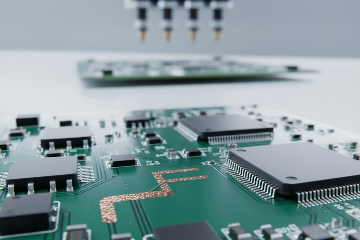
The most direct way to prevent assembly-induced detuning is to enforce a strict keepout zone around the antenna. This is a defined three-dimensional volume where no conductive materials, components, or assembly tooling are permitted. The rationale is rooted in the physics of near-field electromagnetic coupling.
The Physics of Proximity Effects
An antenna radiates energy through a near-field region where its electric and magnetic fields are reactive, storing and releasing energy. The antenna’s input impedance is highly sensitive to any materials present in this zone.
When a conductive object like a component lead, a solder joint, or a metallic fixture pin enters the near-field, it couples with these reactive fields and acts as a parasitic element. This alters the effective capacitance and inductance the antenna presents to its transmission line. For a patch antenna, a metallic object within 5 millimeters of its radiating edge can shift the resonant frequency by 50 to 150 MHz. For an inverted-F antenna, a component placed within 3 millimeters of its feed point can change the input impedance by 20 ohms or more. The effect decreases with distance, but for most IoT applications at 2.4 GHz, the keepout zone is defined as 6 to 12 millimeters—a compromise between electromagnetic isolation and efficient use of PCB real estate.
Manufacturing Strategies for Keepout Compliance

Defining a keepout zone in a design file is easy; enforcing it during assembly requires a deliberate manufacturing strategy. At Bester PCBA, enforcement begins with tooling. Assembly fixtures are designed so no pin, vacuum port, or support rail intrudes into the keepout volume, a constraint verified using 3D CAD models. A fixture that violates the keepout by even 2 millimeters can invalidate any RF test performed while the board is fixtured.
Component placement verification is the second layer of enforcement. Automated optical inspection systems are programmed with the keepout boundary as a hard constraint. Any component encroaching on the zone triggers a rejection. This is a hard stop; the board does not proceed to reflow until the error is corrected.
Handling also matters. Operators and automated equipment must not apply mechanical pressure to the PCB near the antenna, as deflecting the substrate can temporarily detune it. For boards with antennas near panel edges, depanelization tooling must be positioned so that shear forces do not propagate through the keepout zone.
Preserving Controlled Impedance Stackup Integrity
An RF trace is a transmission line, not just a wire. Its impedance is determined by its width, the substrate thickness, and the dielectric constant of the core material. If any of these parameters change during assembly, the impedance changes, creating reflections that degrade performance.
Dielectric Constant Stability
A substrate’s dielectric constant is specified at a reference temperature, but reflow soldering subjects the board to peaks of 250°C. Lower-cost FR-4 variants can exhibit a dielectric constant shift of 5% to 8% over this range. For a 50-ohm trace, this can shift the impedance by several ohms, introducing reflections that compound with other discontinuities in the RF path.
At Bester PCBA, we require substrate materials with a dielectric constant stability of ±2% over the reflow temperature range for all RF builds. This is verified through material certification from the PCB fabricator, which must specify the measurement method used; the IPC-TM-650 stripline resonator method is our required standard.
Stackup Documentation and Verification

The physical stackup—the sequence and thickness of copper and dielectric layers—must be precise. For a four-layer board, the distance from a signal trace on the top layer to the ground plane on layer two is critical. A design might call for a 10-mil trace over a 5-mil core to achieve 50 ohms. If fabrication tolerance results in a 6-mil core, the impedance shifts to 53 ohms.
We mandate stackup verification through cross-sectional analysis for all RF builds. If a sample’s measured core thickness deviates from the spec by more than 10%, the entire panel is rejected before assembly begins. Impedance errors baked into the board cannot be corrected later. Reflow profile control is also crucial for stackup integrity. We minimize thermal stress by qualifying RF board profiles with a peak temperature no higher than 245°C and a time-above-liquidus under 60 seconds—tighter constraints than standard profiles.
Low-Residue Processes for RF Zones
Flux is a chemical agent essential for soldering, but its residues are dielectrics with a non-zero loss tangent. When left on or near RF circuits, they introduce measurable losses. The problem is compounded by the fact that flux residues are hygroscopic; they absorb moisture from the air, and water is a high-loss dielectric. A thin layer of moist flux residue can increase losses in the antenna’s near-field by an order of magnitude.
Flux Chemistry and Cleaning Protocols
No-clean fluxes, the industry standard, are designed to leave benign residues for most applications. RF circuits are not most applications. Even a thin film from a low-residue no-clean flux can increase dielectric loss, reducing radiated efficiency by 1 to 2 dB.
Our process for RF builds starts with low-residue, low-halide no-clean flux, but we don’t stop there. We implement a targeted cleaning process for RF-critical zones. After reflow, boards are cleaned with isopropyl alcohol and deionized water in an inline system, with nozzles directed at the antenna and RF traces. We verify cleaning effectiveness through ionic contamination testing, enforcing a maximum level of 5 µg/cm², which is twice as strict as the IPC-A-610 class 3 limit.
Solder mask uniformity is another factor. As a dielectric material, variations in its thickness can alter impedance. We specify a solder mask thickness tolerance of ±10 microns for RF zones and verify it during incoming PCB inspection.
Validating Performance with Proper Test Jig Design
Manufacturing controls are only effective if their outcomes are verified. For RF assemblies, this means measuring radiated performance—return loss, radiation pattern, and efficiency—after assembly. The challenge is that the test fixture itself can become a source of detuning.
Radiated Metrics That Matter
Return loss is the most common RF measurement, showing the power reflected from the antenna due to impedance mismatch. A value of –10 dB or better is a typical acceptance criterion. But good return loss doesn’t guarantee good radiation. An antenna can efficiently accept power but convert it to heat due to near-field losses.
Radiated efficiency—the ratio of power radiated to power accepted—is the true measure of performance. Measuring it requires a radiated test in an anechoic chamber, reverberation chamber, or near-field scanner. For production, near-field scanning or reverberation chambers are the most practical methods. A distorted radiation pattern, which creates nulls in critical directions, is another failure mode that must be checked.
Fixture Design That Preserves the Fields

A test fixture must not alter the antenna’s electromagnetic environment. Any metallic support rails or grounding clips in the near-field will couple to the antenna and shift its resonance. At Bester PCBA, our RF test fixtures are designed with strict principles. First, all fixture materials within one wavelength of the antenna are non-metallic, such as PEEK or polycarbonate. Second, power and ground connections are made via spring-loaded pins located far from the RF circuitry. Third, the coaxial cable connecting to the antenna feed is routed away from the structure and dressed with ferrite suppressors to prevent its shield from radiating and distorting the measurement.
We validate every fixture by comparing measurements of a golden sample board in free space versus in the fixture. If the fixture introduces more than 0.5 dB of error or shifts the resonant frequency by more than 20 MHz, it is redesigned.
Finally, every board is serialized, and its test data is logged in our manufacturing execution system. This traceability allows for rapid root cause analysis if a field failure ever occurs.
Manufacturing Discipline Is RF Performance Insurance
These four disciplines are not independent safeguards. They are a system. Keepout enforcement is useless if the substrate’s dielectric constant shifts during reflow. A perfect impedance stackup doesn’t matter if flux residue is killing efficiency. A clean board can’t be validated if the test fixture detunes the antenna.
Achieving RF performance that survives assembly requires systematic enforcement of all four disciplines on every build. A lapse in any one area compromises the entire effort. This isn’t paranoia; it’s engineering rigor. Most RF assembly failures trace back to an incomplete implementation of these controls: keepout zones defined but not enforced in tooling, stackups specified but not verified, or return loss measured in an unvalidated fixture.
The cost of these controls is modest—typically adding 50 cents to 2 dollars per board. The cost of not implementing them is field failures, product recalls, and a damaged reputation. The return on investment is unambiguous. At Bester PCBA, we don’t treat RF assembly as a special case. If your design has an antenna, our process includes these disciplines by default. The outcome is RF performance that matches the design intent, validated by measurement, and delivered with the consistency that volume production demands.


