Circuit boards, or Printed Circuit Boards (PCBs), are integral to the functioning of virtually all electronic devices. They provide the foundation for arranging electronic components in a compact and efficient manner. This article aims to delve into the working principles of circuit boards, their structure, and the main causes of faults that can occur during their operation.
Working Principle of Circuit Boards
The working principle of a circuit board is based on the use of an insulating substrate material to separate the conductive copper foil layer. This arrangement allows the electric current to flow along a predetermined route, enabling various components to perform functions such as amplification, attenuation, modulation, demodulation, and coding.
Structure of Circuit Boards
A circuit board is primarily composed of pads, through-holes, mounting holes, wires, components, connectors, fillings, and electrical boundaries. The common types of circuit boards based on their layer structure include Single-layer Boards (single-layer PCB), Double-layer Boards (double-layer PCB), and Multilayer Boards (multi-layer PCB).
Components of Circuit Boards
Each component of a circuit board serves a specific function:
- Solder Plate: This is a metal hole used for soldering component pins.
- Through-hole: These can be metallic or non-metallic. Metallic through-holes are used to connect the component pins between each layer.
- Mounting holes: These are used for fixing the circuit board.
- Conductor: This is the electrical network copper film used to connect the pins of the components.
- Connectors: These are used for connecting components on the circuit board.
- Filling: This is the deposited copper for the ground network, which can effectively reduce impedance.
- Electrical boundary: This is used to determine the size of the circuit board. All components on the circuit board must not exceed this boundary.
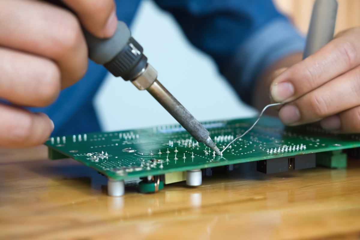
Causes of Welding Defects in PCBs
Welding defects in PCBs can be attributed to several factors. One of the primary reasons is the solderability of the circuit board hole. Poor solderability can lead to virtual welding defects, affecting the parameters of the circuit components. This can result in instability in the conduction between multilayer board components and inner-layer wires, causing the entire circuit to fail.
Factors Affecting Solderability
The main factors affecting the solderability of printed circuit boards are:
Composition and Nature of Solder
Solder is an essential part of the chemical process of welding. It consists of chemical materials containing flux. The common low melting-point eutectic metal is Sn-Pb. The impurity content must be controlled to prevent impurities from being dissolved by the flux. The function of the flux is to help solder wet the surface of the solder plate circuit by passing heat and removing rust. White rosin and isopropyl alcohol solvent are generally used.
Welding Temperature and Surface Cleanliness
When the temperature is too high, the diffusion speed of solder at this time has very high activity. This can cause the circuit board and the surface of the solder to oxidize rapidly, resulting in welding defects. Contamination on the circuit board surface can also affect weldability and thus create defects. These defects include tin beads, tin balls, open circuits, and gloss.
Understanding the structure and working principle of circuit boards, as well as the factors that can lead to welding defects, is crucial in the manufacturing and maintenance of electronic devices. By addressing these issues, we can ensure the reliable and efficient operation of our devices.

 PCB Technology: Types, Benefits, Challenges, and Applications")


