A conformal coating is the armor for a printed circuit board (PCB), protecting it from moisture, dust, and chemicals. But that armor creates an insulating barrier over every surface it touches. A coated test pad becomes an inaccessible test pad.
When functional testing relies on probe contact, or when future repairs require desoldering components, the decision to coat without proper masking is critical. Get it wrong, and a protected board becomes an untestable, unrepairable brick. The choices made during masking and coating determine whether a product remains serviceable throughout its lifecycle or becomes e-waste the first time a component fails.
At Bester PCBA, we don’t treat masking and coating as a final checkbox. It’s a deliberate process of selecting methods, controlling thickness, and documenting design choices that directly impact a product’s long-term value. The central conflict is straightforward: complete coverage provides maximum environmental protection, but it also eliminates the access points needed for testing and repair. Solving this requires a deep understanding of how masking methods differ in precision, how coating thickness affects reliability, and how early design choices prevent costly problems later.
Why Test Pad Access Defines Success

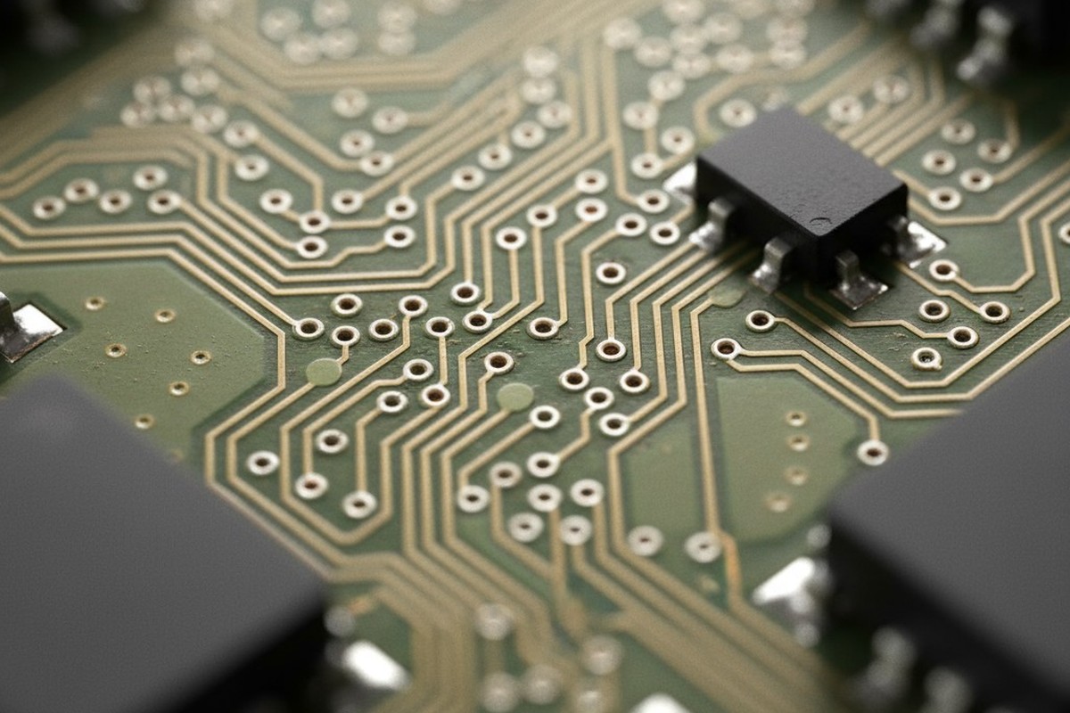
Test pads are the designated electrical windows into a circuit, essential for in-circuit tests, flying probes, boundary scans, and manual troubleshooting. These exposed copper areas are designed for temporary contact. When a conformal coating seals them off, it creates a physical and electrical barrier that blocks test probes. The result is a board that cannot be verified after coating, allowing functional defects to go undetected until the product is in a customer’s hands.
The consequences ripple beyond the factory floor. A board that passes its initial tests but fails in the field cannot be diagnosed if its test points are sealed. Technicians are left with two bad options: attempt to scrape away the coating, which risks damaging traces and contaminating the board, or replace the entire assembly without ever knowing the root cause. The first adds labor and quality risk; the second adds material cost and forfeits the chance to perform failure analysis.
Rework and repair face the same barrier. Replacing a failed component often requires access to adjacent test points to verify the fix or repair damaged traces. If those pads are coated, a technician must meticulously remove the coating without damaging the surrounding area—a time-consuming and error-prone task. In high-reliability or high-volume production, the cumulative cost of these rework complications often dwarfs the initial cost of precision masking. An entire production run with poor masking can grind to a halt at functional test, forcing a choice between scrapping thousands of boards or reworking every single one.
The Conformal Coating Challenge
Conformal coating is a thin polymer film applied to a PCB to shield it from environmental stress. It’s a barrier against moisture, dust, chemicals, and even salt spray in harsh marine or industrial environments. The coating flows over the board’s topography, covering components, solder joints, and traces. This complete coverage is the goal, as any gap becomes a potential entry point for contaminants that cause corrosion or electrical shorts.
This need for a perfect seal creates the fundamental conflict with testability. A test pad must remain conductive and accessible. A conformal coating is, by definition, an insulator. When it covers a test pad, it raises the surface resistance and physically blocks the metal-to-metal contact a test probe requires. Even a thin layer can cause intermittent contact or complete test failure, especially in high-frequency or low-current circuits where contact integrity is paramount.
The solution isn’t a different material—all conformal coatings, whether acrylic, silicone, urethane, or parylene, are insulators. The only way to preserve test pad function is to prevent the coating from reaching them. This is the job of masking: to create precise exclusion zones on the board. The quality of the masking method directly determines whether a board remains testable after it’s protected. As board density increases, with test pads squeezed between components or under connectors, the challenge intensifies, demanding masking methods that can deliver precision without compromising protection.
Custom Boots vs. CNC Masking
The choice of masking method is a trade-off between setup cost, per-unit labor, and precision. For production, two methods dominate: manually applied custom silicone boots and programmatically controlled selective coating. Each has a distinct profile, and the right choice depends on production volume, board complexity, and cost targets.
Custom Silicone Boots and Manual Masking

Custom silicone boots are small, flexible caps molded to fit over specific test pads. Placed on the board before coating and removed after it cures, they act as simple physical barriers, leaving the pads clean and accessible. The concept is straightforward, requiring no specialized equipment beyond the boots themselves and the labor to handle them.
The main advantage is low setup cost. For prototypes or low-volume runs, the only investment is in the custom molds and the labor time. This makes boots an economical choice for small batches or boards with simple layouts where pads are large, widely spaced, and easily accessible.
However, the limitations appear as production scales. Placement and removal are manual, adding labor cost to every single board. For a board with just ten test pads, an operator might spend several minutes per board on masking alone. In a run of 1,000 boards, that translates to dozens of hours of labor. The per-unit cost never goes down.
Precision is another constraint. A boot must fit snugly to prevent coating from wicking underneath, yet be removable without leaving residue or pulling up the pad. This is a difficult balance, especially with varied pad sizes or tight component spacing. Boots are also useless for test pads in recessed areas or under components. This method works best when a design accommodates it, but fails when precision is paramount.
CNC-Controlled Selective Coating
Computer Numerical Control (CNC) masking doesn’t block coating; it controls exactly where it’s applied. Instead of a blanket spray, a CNC-controlled dispensing system follows a precise toolpath generated from the board’s CAD data. It deposits coating only in approved areas, programmatically creating exclusion zones around test pads, connectors, and mounting holes with sub-millimeter accuracy.

The initial setup cost is higher. It requires CAM programming to generate the toolpath, verification to ensure alignment, and potentially custom fixtures. This may take several hours of engineering time. But once the program is validated, the per-unit cost plummets. The process is automated, with cycle time determined by machine speed, not manual labor.
This inverted cost structure makes CNC masking dominant at higher volumes. The setup cost is amortized across the entire run, and the break-even point against manual boots often occurs in the low hundreds of units. Beyond that, CNC becomes far more cost-effective.
More importantly, CNC masking offers a qualitative leap in precision. Exclusion zones are defined with positional accuracy often better than 0.5 millimeters, enabling the masking of tiny pads tucked between components—geometries impossible to handle with boots. The repeatability is flawless; every board is coated identically, eliminating the variability of manual work. This precision allows designers to minimize keepout zones, maximizing the board’s protected area. If a design includes pads under components or smaller than 1 millimeter, CNC masking is often the only viable option.
UV Thickness Control and Defect Prevention
Applying the coating is only half the battle. Ensuring it has the correct thickness and is free of defects determines whether it offers real protection or introduces new failure modes. The goal is not a single thickness value, but a controlled range—too little coating leaves the board vulnerable, while too much creates internal stress that can cause cracking, delamination, or lift-offs.
Why Coating Thickness Dictates Reliability
An effective conformal coating must meet a minimum thickness, typically 25 to 75 micrometers, to provide a complete barrier. A coating that’s too thin has microscopic pinholes where moisture can penetrate and begin corrosion. This is a common problem at the sharp edges of traces or around component leads, where liquid coating can pull away.
Excessive thickness creates a different set of problems. As the coating cures, it shrinks, generating internal stress. If the coating is too thick, these forces can exceed its adhesion to the board, causing it to peel away or delaminate. This failure often starts at the sharp edge of a masked area. Thick coatings are also more brittle and prone to cracking under the stress of thermal cycling, as the board and components expand and contract at different rates.
The optimal thickness is therefore a balance: robust enough for environmental protection, but thin enough to remain flexible and stress-free. Achieving this balance requires measurement, not estimation.
Measuring with UV Fluorescence

Many conformal coatings are formulated with a UV-fluorescent additive, providing a simple, non-destructive way to verify coverage. Under a UV lamp, the coating glows with an intensity proportional to its thickness. A thin layer appears dim, while a thick layer is bright. This allows an operator to instantly spot uneven coverage, thin spots in the shadows of tall components, or excessive buildup.
The inspection is quick but reveals defects invisible in normal light. The transition zones around masked areas are especially critical. A gradual “feathering” of the coating edge distributes stress, while a thick, steep ridge is a prime location for delamination. UV light also exposes other defects like air bubbles or “fisheyes” where the coating failed to adhere due to surface contamination.
While UV inspection is qualitative, it provides enough resolution to catch process deviations and ensure thickness is within an acceptable range. For absolute measurements, other tools exist, but for most applications, a trained eye under a UV lamp is the first line of defense. The foundation for this, however, is a perfectly clean surface. Any flux residue, oil, or particulate left on the board before coating will compromise adhesion, trapping a failure point directly beneath the protective layer.
Designing for Rework
The ability to rework a coated board is not a matter of luck; it’s the result of deliberate design and documentation choices made long before production begins. A board designed for rework has ample space for tools, uses robust test pad geometries, and is documented with clear masking instructions.
Test Pad Sizing and Spacing: A pad that needs to remain accessible should be large enough for a technician to work on, ideally at least 1.5 to 2 millimeters. This provides enough area to remove any coating encroachment without accidentally cutting a trace or lifting the pad. Similarly, a keepout zone of at least 1 millimeter around test pads gives tools clearance from adjacent components, reducing the risk of collateral damage.
Clear Documentation: The manufacturing files must be unambiguous. The board data should include a dedicated coating mask layer in the Gerber or ODB++ files that explicitly defines every exclusion zone. Leaving this to interpretation on an assembly drawing invites inconsistency and error, especially as production scales or moves between vendors.
Rework Strategy: When a component fails, the coating over its leads must be removed. The method depends on the material. Acrylics dissolve with solvents. Silicones and urethanes require careful mechanical abrasion or thermal softening. Parylene, the toughest of all, often needs micro-abrasion or laser ablation. In every case, the risk is damage to the board. The safest process is slow and precise, performed by a trained technician.
After the component is replaced, the area must be recoated by hand to restore protection. This new coating must adhere well to the old layer without creating a thick, stressful boundary. The success of this entire procedure—from removal to reapplication—hinges on the foresight of the original design. Boards with large, accessible test pads and clear masking instructions can be reworked with confidence. Those without become a high-risk gamble.

 Circuit Board Assembly")


