Every printed circuit board begins its life as a standardized sheet of laminate, usually copper-clad FR4. This is the only fundamental truth in the manufacturing process that physics does not allow you to negotiate.

When a design file arrives at the fabrication house, the first thing the CAM engineers do is attempt to fit your arbitrary dimensions onto this fixed canvas. If your board is 100mm by 100mm, they might fit twelve units on a sheet. If you designed it to be 98mm by 98mm, they might fit sixteen. That single decision—often made arbitrarily by a designer staring into an empty CAD void rather than at a factory floor—just increased the unit cost by thirty percent.
You are paying for the air. In the industry, we call it “off-cut” or “web waste,” but functionally, it is money you paid for that the fab must then pay a disposal service to haul away. The pricing model for PCBs isn’t linear based on the square inch of the final board; it is a step-function based on how many units survive the cut from the master sheet. The most expensive material in your product is often the stuff that ends up in the trash can behind the routing machine.
The Fundamental Constant
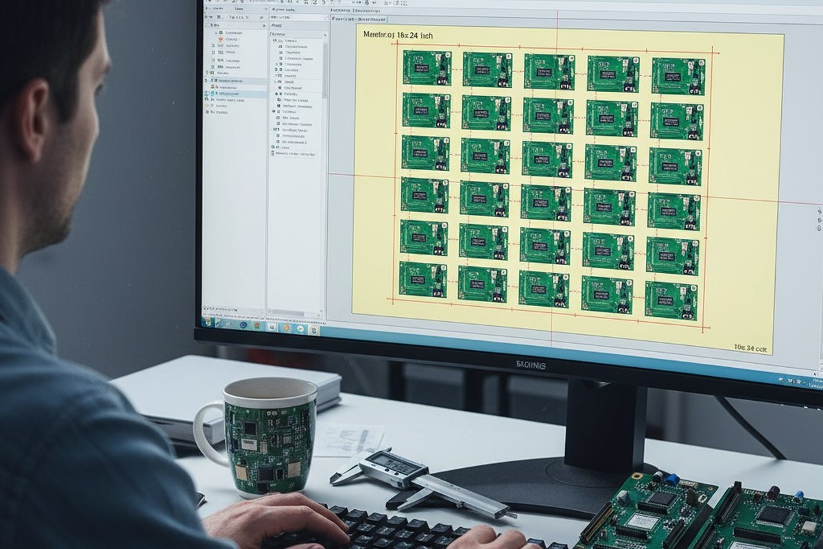
The universe of electronics manufacturing revolves around the 18-inch by 24-inch laminate sheet. While larger formats like 21×24 exist, and massive volume runs (think 500k units) might justify a custom web size from the supplier, the 18×24 sheet is the hard ceiling for the vast majority of production.
But you do not get to use all of it. This is where “working area” confusion destroys profit margins. A designer often assumes they have 18 inches of width to play with. They don’t. The fabrication machinery needs to grip the edges of the panel to dip it into plating baths and transport it through etching lines.
These “handling margins” usually consume a full inch of the perimeter: half an inch on all four sides. This shrinks your usable reality from 18×24 down to a 16×22 working area. If your panel design requires 16.5 inches of width, you have just forced the fab to rotate the array or drop to a smaller, less efficient standard size, instantly spiking the waste percentage.
It is critical to distinguish between “Prototype Mode” and “Production Mode” here. A prototype shop might sell you a “fixed price” for a few boards and eat the waste cost themselves to win your business. They are subsidizing your inefficiency. When you move to production volumes of 10k or 50k units, that subsidy vanishes. You are billed for every square inch of the master sheet, utilized or not.
The Invisible Tax of Tooling
Once you accept the boundaries of the sheet, you must account for the space between the boards. In a CAD tool, it is easy to place two PCBs zero millimeters apart. In the physical world, cutting tools have mass and width.
If you choose to route your boards out of the panel—physically cutting them free—you must leave room for the router bit. The standard bit width in most Shenzhen or domestic fabs is roughly 2.4mm (about 100 mils). We call this the “kerf,” the path of destruction the tool carves out as it travels.
If you have a 10×10 array of small sensor boards and you rely on routing, you are introducing ten vertical and ten horizontal channels of 2.4mm empty space. Across a panel, that adds up to inches of lost laminate—space that could have hosted two or three more revenue-generating units. Depanelization isn’t just a mechanical constraint; it’s a financial lever.
The alternative is V-scoring. This process cuts a groove into the top and bottom of the board, leaving a thin web of material to hold it in place until assembly is finished. Crucially, V-scoring requires essentially zero spacing between boards. You can butt them right up against each other.

However, V-scoring is a blunt instrument. It can only cut straight lines across the entire length of the panel; it cannot stop halfway. If your board has hanging connectors, complex curves, or components overhanging the edge, V-scoring is physically impossible. You are forced back to the router, and you are forced to pay the 2.4mm tax.
Do not forget the rails. The assembly house—the folks putting the chips on the board—needs “waste rails” on the edge of the panel to transport it through the SMT line. These rails are usually 0.5 inches (12.7mm) wide. They contain the fiducials (optical targets for the pick-and-place cameras) and tooling holes. You pay for this laminate, but it will never be part of a sold product. It is a necessary structural evil.
The Math of the Millimeter
Consider a generalized scenario that plays out in quoting departments every day. Imagine a client requests a board for a consumer IoT device. The mechanical engineer, prioritizing a specific enclosure aesthetic, locks the PCB dimensions at 98mm by 98mm.
The fab receives the files. They apply the handling margins to the standard 18×24 sheet. They account for the 10mm waste rails for assembly. They factor in the 2.4mm router spacing because the board has rounded corners (an aesthetic choice).
The result? The fab can fit exactly six boards on a working panel. The utilization is poor—maybe 55%. The rest is trash.
Now, look at the geometry. If that board were 96mm instead of 98mm—a reduction of just 2mm—the CAM engineer could rotate the array. Suddenly, the math shifts. They can nest the boards differently. They can fit eight boards on that same panel.
That is a 33% increase in yield from the exact same sheet of raw material. The cost of the laminate, the copper, the solder mask, and the machine time is effectively divided by eight instead of six. That 2mm reduction drops the unit price by roughly $0.40. On a 100,000 unit run, that is $40,000 of pure profit found in a 2mm sliver of FR4.
This is why you must perform the “Geometry Check” before freezing the mechanical constraints. Take the standard working area (16×22) and divide it by your board dimensions + spacing. If the result is a messy fraction (e.g., 4.2 boards per row), you are in the danger zone. You want integers. You want to fit exactly 5.0 or 6.0 boards.
There is often pushback here regarding aesthetics. Designers love non-rectangular shapes: circles, L-shapes, complex contours. From a manufacturing standpoint, these are the enemies of utilization. An L-shaped board creates a negative space that is often impossible to fill, even with aggressive nesting (flipping every other board 180 degrees). Unless that odd shape is absolutely critical for the product’s function, square it off. The router bit wear and the waste material are costs that provide zero value to the end user.
Structural Integrity & The Assembly Trap
Optimizing for pure density has a breaking point, quite literally. A panel that is packed too tightly, with too much material removed, loses its structural integrity.

During the assembly process, the panel travels on a conveyor through a reflow oven where temperatures hit 250°C. At this heat, the FR4 material softens. If you have “mouse bites” (break-away tabs) that are too weak, or if you have routed away too much supporting material to squeeze in one extra board, the panel will sag.
In the worst cases, the panel snaps inside the oven. This is a catastrophic failure. You lose the PCBs, the expensive components mounted on them, and you potentially damage the assembly machine. It is a classic “penny wise, pound foolish” situation. You saved 5% on laminate utilization but reduced your assembly yield by 10% due to warped or snapped panels.
There is also the question of “X-outs.” In high-volume production, it is statistically probable that some spots on a large laminate sheet will have defects (etching errors, debris). If you demand that every single panel delivered to you must have 100% good boards, the fab has to throw away entire panels just because one unit out of twelve failed. This drives your cost up massively.
If you allow “X-outs”—marking the bad board with a black marker but shipping the rest of the panel—you allow the fab to save the good units. Most contract manufacturers can handle X-outs; their machines simply skip the bad spot. Confirm this with your assembly house, but never forbid X-outs unless you enjoy burning money.
The Final Check
The most expensive time to learn about panelization is after the design is finished. The cheapest time is during the concept phase. Before you lock in a dimension, call the fabrication house. Ask them for their “standard working panel size” and their preferred spacing rules. Do not rely on the defaults in your CAD software, and certainly do not assume that the prototype shop’s specs apply to the production floor.
Take your proposed dimensions, add the 2.4mm router gap (or 0mm for V-score), add the edge rails, and see how many fit into 16×22. If the answer involves a lot of empty space, change the dimension. Physics will not adjust to suit your design; your design must adjust to suit the physics of the sheet.


