It usually happens on a Tuesday afternoon, just as the line is ramping up for a rush order. The pick-and-place machine—maybe a Panasonic NPM or a high-speed Juki—is humming along, the conveyor is moving, and the dashboard metrics are green. Theoretical throughput looks high. The machine is finding the global fiducials on the panel rails without a single error log. According to the coordinate geometry in the placement file, everything is perfect.

Then the boards come out of the reflow oven.
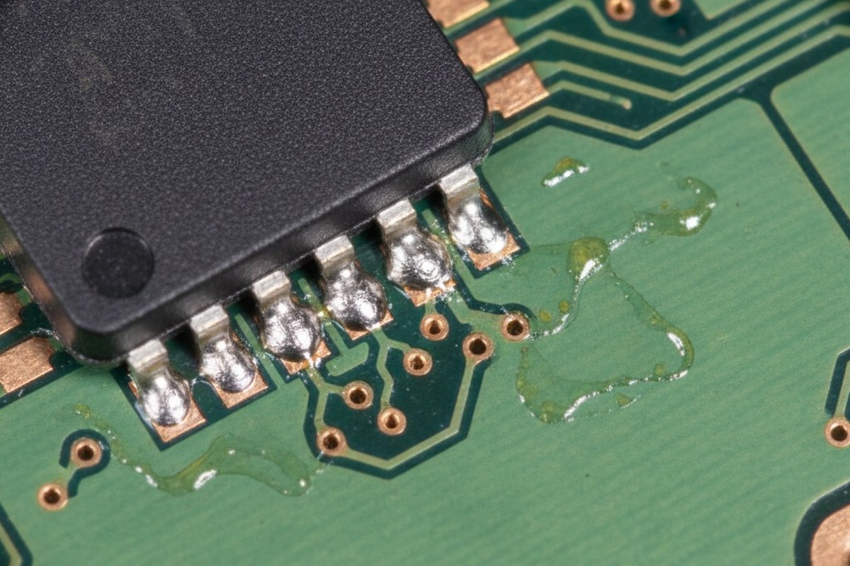
You look under the microscope and see the disaster. Every single 0.4mm pitch QFN is shifted 0.15mm to the left. The pads are bridged. The 0201 passives are tombstoned or skewing off their landing zones. You are holding a panel of expensive confetti.
The project manager wants to know why the machine failed. But the machine didn’t fail. It did exactly what it was told based on the references it was given. The failure happened weeks ago, inside a CAD software suite, when a designer decided that three fiducials on the panel rails were “good enough” for the entire assembly.
The Geometry of the Lie
There is a fundamental misunderstanding in PCB design that treats the board as a rigid, immutable grid. In the CAD environment, the distance between the origin point (0,0) and a component pad at (250, 150) is a mathematical absolute. It never changes.
On the factory floor, that grid is a lie.
When a machine clamps a panel, it looks for the global fiducials—those copper circles usually sitting on the waste rails or the board corners. It calculates the board’s position based on those points. If the board is rotated slightly—a “theta” error—the machine compensates mathematically, rotating its internal coordinate system to match the board.

The problem is that geometry leverages error over distance. A rotational error of just 0.05 degrees at the rail might result in a negligible shift for a component 10mm away. But for a component sitting in the center of a 300mm panel, that same tiny angular error translates into a massive lateral swing. The machine thinks it is placing the part at the perfect coordinate, but because the reference point is so far away, the “lever arm” of the error amplifies the drift.
You are asking a machine to thread a needle from across the room based on a map someone drew on a napkin. It doesn’t matter if the machine brochure claims 30-micron accuracy. That accuracy is relative to the reference it sees. If the reference is on the rail and the target is 150mm away, you are fighting trigonometry, and trigonometry always wins.
FR-4 is a Living Sponge
The geometric leverage is bad enough, but it assumes the board itself is stable. It isn’t. We tend to think of PCBs as steel plates, but they are composites of woven glass and epoxy resin. They are closer to a stiff fabric than machined metal.
FR-4 is a living, moving material. It breathes with temperature. When you run a double-sided assembly, that board goes through a reflow oven for the first side, seeing temperatures upwards of 240°C. The material expands. The glass fibers hold tension. The resin cures further. When it cools down, it does not return to its exact original dimensions. It shrinks, warps, and twists.
If you are dealing with flexible circuits or polyimide materials, this reality is even more violent. A flex panel can stretch non-linearly, meaning one corner might expand by 0.1mm while the center expands by 0.3mm.
From the machine’s perspective, this is a nightmare. It reads the rail fiducials, measures the distance between them, and notices the board has shrunk by 0.5mm over its length. High-end machines from ASM or Mycronic have “shrinkage compensation” algorithms that try to average this error out across the board by scaling the placement coordinates.
But this scaling assumes the distortion is linear—that the board stretched evenly like a rubber band. In reality, the board distorted like a wet sponge drying in the sun. The local distortion near that fine-pitch BGA in the center might be completely different from the distortion near the edge connectors. The machine, looking only at the rails, has no way of knowing this. It applies a global fix to a local problem.
This is also why you see stencil alignment issues that mimic placement errors. If your stencil printer is aligning to those same rail fiducials, it is also guessing where the pads are. You end up with solder paste deposited half-on, half-off the pad, and the component placed half-on, half-off the paste. The result is a guaranteed reflow defect.
The Local Fix

There is only one way to defeat the physics of distortion and the geometry of leverage: Local Fiducials.
A local fiducial is a reference mark placed immediately adjacent to the fine-pitch component. By “adjacent,” we mean inside the same functional block, often within 10-20mm of the target.
When you force the machine to use local fiducials, you change the game. The machine moves the camera to the component area, finds the local marks, and resets its origin point. Now, the “lever arm” of any rotational error is practically zero. The machine doesn’t care if the panel rail is 5mm off, or if the board warped 1mm over its length. It only cares about the relationship between those local marks and the pads right next to them.
This creates a “truth window” around the component. Inside that window, the relative accuracy is extremely high because the reference is immediate.
Designers often push back on this. They argue they don’t have the space. They want to save that 1mm x 1mm square for a trace or a via. But you have to ask: what is the cost of that space versus the cost of rework? If you are placing a 0.4mm pitch QFN, a 0.5mm pitch BGA, or a high-density connector, you aren’t negotiating with an operator; you’re fighting math.
The rule of thumb is simple: If the component pitch is 0.5mm or less, it requires local fiducials. If the component is a BGA with more than 400 pins, it requires local fiducials. Two marks are required to correct for rotation—usually placed diagonally across the component body. One mark is useless for rotation; it only gives you translation (X/Y).
Designers’ Favorite Shortcuts (That Don’t Work)

When told they need local references, clever designers often try to cheat the system. The most common attempt is the “Via as Fiducial.”
They will point to a via near the component and ask, “Can’t you just tell the camera to look at that hole?”
No.
A mechanical drill bit wanders. The tolerance on a drilled hole position is often +/- 0.1mm or worse, depending on the fab house’s drill stack. Furthermore, the plating around the hole can be irregular. A machine vision system works on contrast—specifically, the contrast between the shiny copper/gold/solder and the dark soldermask. A via is a messy optical target. It has depth, shadows, and irregular edges.
Using a via as an alignment point is like trying to calibrate a sniper rifle using a target painted on a balloon blowing in the wind. You are introducing more error into the system than you are removing.
Similarly, do not rely on the soldermask openings of the pads themselves. Soldermask registration tolerance is loose (around +/- 75 microns). The copper pad is the only thing that matters electrically, so the alignment mark must be etched in the same copper layer as the pad. That is the only way to guarantee they move together.
The Bottom Line
This isn’t about how to set these up in your CAD software—that’s a tutorial you can find elsewhere. This is about the survival of your production run.
Global fiducials on the rails get the board into the machine. They handle the coarse alignment required to transport the panel and place the large, forgiving parts like electrolytic capacitors or big inductors.
But local fiducials get the part onto the pads. They are the only defense against the warping, twisting, and stretching reality of the manufacturing process. Omitting them to save space is false economy. You save a millimeter of FR-4, but you pay for it with hours of technician time, X-ray inspection costs, and the “expensive confetti” of a scrapped panel.
Design for the reality of the material, not the perfection of the grid.


 Circuit Board Assembly")

