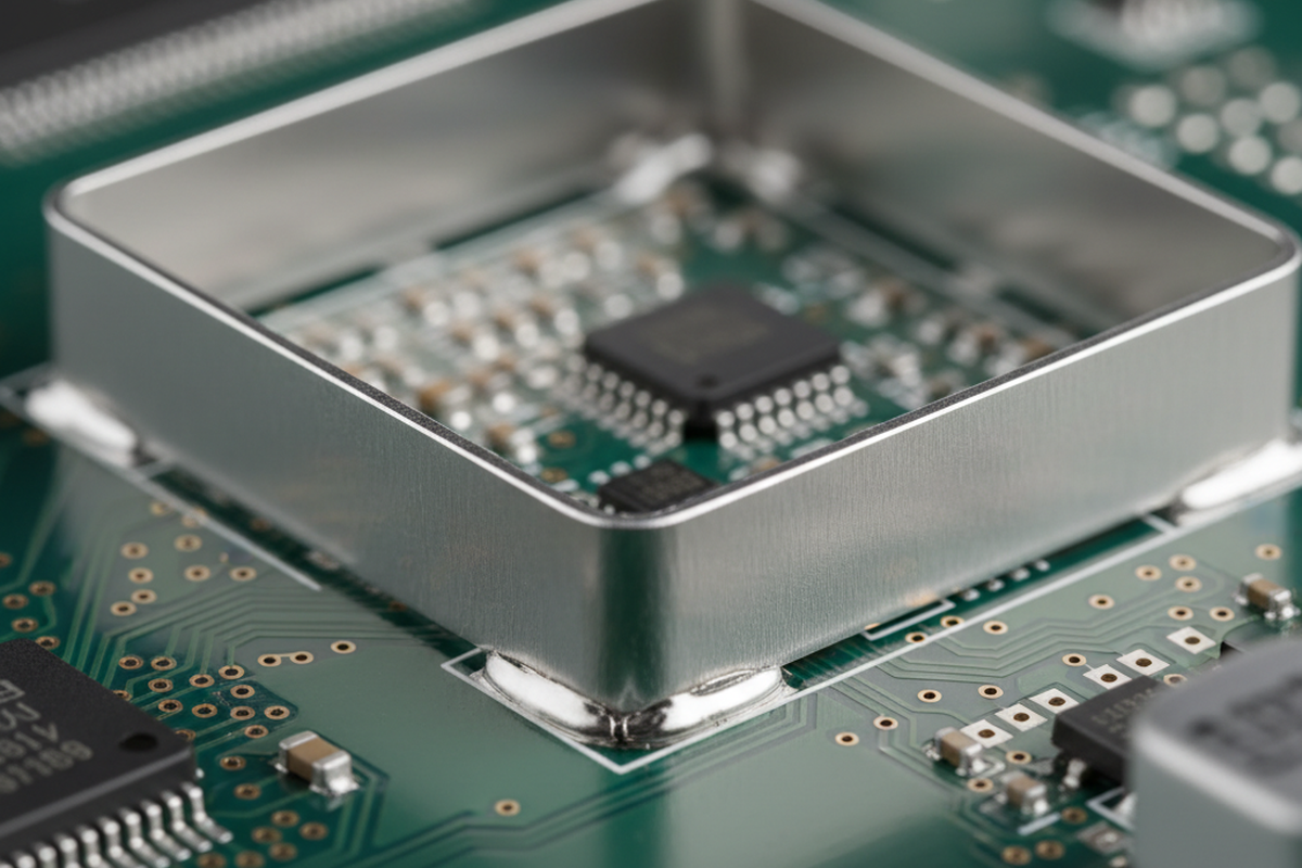
The most dangerous component on a mixed-signal PCB isn’t the BGA, nor is it the QFN with the thermal pad. It’s the RF shield can. While engineers spend weeks simulating impedance matching and antenna tuning, the physical shield itself is often dropped onto the layout as an afterthought—a simple metal box drawn with a solid line of solder paste on the mechanical layer.
That “afterthought” is a manufacturing time bomb. When a production line shuts down because 15% of boards are failing vibration testing, or when a 0201 capacitor mysteriously shorts out three months after deployment, the culprit is almost always the shield assembly process. The issue rarely stems from shielding effectiveness itself. It stems from the refusal to acknowledge that a shield is a massive thermal heatsink and a gas trap. If you design a shield footprint without respecting the fluid dynamics of molten solder, you aren’t building a Faraday cage. You are building a bead generator.
The Invisible Enemy: Solder Beading
The failure mechanism is simple, violent, and microscopic. When you print a standard solid line of solder paste for a shield frame, it creates a wet seal against the PCB surface. During reflow, the flux inside that paste becomes volatile and needs to vent. In a typical component joint, the gas escapes around the edges. But under a heavy shield wall with a continuous bead of paste, the gas is trapped.
Pressure builds until it effectively explodes, ejecting tiny spheres of molten solder out from under the shield wall. These are “solder beads.” In the worst cases—often seen in high-volume automotive runs—these beads float across the board surface on a cushion of flux. They eventually lodge themselves underneath nearby components, like 0201 passives or fine-pitch IC pins, creating a hard short. Because the bead is often wedged under the component body, standard Automated Optical Inspection (AOI) will miss it. Even X-ray inspection isn’t a cure-all; on a dense board with ground planes, a small solder bead can easily hide in the noise. The only real fix is preventing the bead from forming in the first place.
Aperture Engineering: The 1:1 Fallacy
The most common error in shield design is a 1:1 relationship between the copper pad and the stencil aperture. If the pad is 1mm wide, the engineer requests a 1mm wide paste deposit. That is a mistake. A shield doesn’t need a hermetic solder seal to function as an EMI blocker; it requires electrical continuity and mechanical fixation.

To eliminate beading, you must break the seal. The stencil aperture should never be a solid line. Instead, it must be segmented. Standard IPC-7525 guidelines and practical experience on the SMT line point to a “dashed line” or “window-pane” pattern. By breaking the paste deposit into segments with small gaps (typically 0.3mm to 0.5mm), you provide a chimney for flux volatiles to escape. This reduces the hydraulic pressure during reflow and keeps the solder where it belongs.
Designers often push back here, fearing RF energy will leak through the gaps. For standard commercial frequencies (sub-6GHz), this is largely a myth. The signal wavelength is vastly larger than the 0.3mm gap in the solder. Unless you are working in extreme millimeter-wave applications, the physics of the wave won’t permit it to pass through such a small aperture. The risk of a short circuit from a solder bead is a 100% functional failure; the risk of RF leakage from a segmented solder joint is statistically negligible. Prioritize the yield.
Furthermore, you need to reduce the volume of paste. A shield sits on top of the solder; it doesn’t have leads that “sink” into it. A 1:1 volume often causes the shield to float or tilt (loss of co-planarity). Reducing coverage to 50-60% of the pad area is usually the sweet spot. For extremely sensitive layouts, using a “reverse home plate” aperture shape can pull excess solder away from the inner edge of the shield, further reducing the chance of internal beading.
Architecture: The “Black Box” Problem
Beyond the stencil, the physical architecture of the shield dictates device reliability. There is a strong temptation to use one-piece shields (a single stamped metal can soldered directly to the board) because they are cheaper and have a lower profile. However, a one-piece shield turns the underlying circuit into a black box.
Once that can is soldered down, visual inspection is impossible. More critically, cleaning is impossible. If you use a water-soluble flux, or even a “no-clean” flux in a humid environment, you have to consider what happens to the residues trapped under that can. If the shield has a near-zero standoff height, wash chemistry cannot flow underneath it. The flux residue remains active, pooling around sensitive traces. Over time—especially in wearable or medical devices exposed to body heat and moisture—this residue leads to dendritic growth and electrochemical migration. The circuit eats itself.
If reliability is paramount, use a two-piece system: a fence (frame) soldered to the board, and a snap-on lid. This allows for full visual inspection of the reflowed joints and thorough cleaning of flux residues before the lid is snapped on. Yes, the Bill of Materials (BOM) cost is higher. But the cost of scrapping a finished board because a $0.05 regulator failed inside a sealed can—requiring a heat-gun rework that lifts pads and destroys the PCB—is infinitely higher.

For prototyping or boards requiring frequent access, consider SMT shield clips. These small spring contacts hold a can in place without a continuous solder ring. They eliminate the beading risk entirely because there is no long line of paste, and they allow for easy removal of the shield during debugging. While they may not provide the same vibration resistance as a soldered frame for aerospace applications, they are often superior for consumer electronics where reworkability is a hidden requirement.
The Thermal Soak
Then there is the thermodynamics of the reflow oven. A metal RF shield is essentially a heatsink. It has a high thermal mass compared to the tiny resistors and capacitors surrounding it. If your reflow profile is aggressive—ramping up heat quickly—the small components will reach liquidus temperature long before the shield does.
This leads to “cold joints.” The solder paste on the shield pads may melt, but the shield wall itself isn’t hot enough to accept the solder. The flux burns off, the paste wets to the PCB pad, but it fails to wet the nickel-plated shield wall. You end up with a shield sitting in a pool of cold solder rather than being bonded to it. Under thermal cycling or mechanical shock, these joints crack instantly.
To counter this, the reflow profile requires a substantial “soak zone”—a period where the oven temperature holds steady (usually between 150°C and 180°C) for 60 to 90 seconds. This allows the thermal mass of the shield to catch up with the rest of the board. You cannot simply blast the board with heat; you must let it soak until the metal of the shield is hot enough to wet. This might slow down the line’s Units Per Hour (UPH), but it ensures the joint is metallurgical, not just cosmetic.
The Process Control Checklist
To build a shield that doesn’t kill your yield, follow this hierarchy of defense:
- Segment the Aperture: Never print a solid line of paste. Use a dashed pattern with 0.3mm-0.5mm gaps to allow outgassing.
- Reduce Volume: Target 50-60% paste coverage relative to the pad area.
- Respect the Mass: Ensure the reflow profile has a soak zone long enough to heat the shield wall, not just the paste.
- Design for Reality: If you cannot clean under it, assume corrosion will happen unless you validate the flux and the environment perfectly. Prefer two-piece systems or clips whenever the budget allows.
Physics is indifferent to your deadlines. If you trap gas, it will explode. If you steal heat, the solder won’t bond. Design the process, not just the schematic.


 Circuit Board Assembly")
