The reflow oven completes its thermal profile, the boards emerge from the vapor phase, and the RF shields sit cleanly soldered to their pads. The assembly looks flawless. Three weeks into functional testing, however, intermittent failures begin to surface. When you remove the shield, the evidence is unmistakable: tiny solder balls scattered across the board, trapped moisture stains radiating from vias, and in the worst cases, solder bridges shorting traces.

The root cause? A design decision that seemed conservative, a standard practice borrowed from general PCB design without considering the unique environment under a shield. That decision was via tenting.
While tenting vias makes sense in many contexts, the enclosed space under an RF shield transforms the reflow process into a pressure vessel experiment. Trapped moisture, volatiles in the solder mask, and the breakdown products of epoxy resin all seek escape routes as temperatures spike. With a metal can sealed to the board, those routes are few. The consequences show up as outgassing damage, solder ball defects, and compromised reliability. We argue that via tenting should be avoided entirely under and immediately adjacent to RF shields. The case against it is rooted in the physics of reflow and the material behavior of solder mask under thermal stress.
The Common Practice Hiding a Reflow Bomb
Via tenting, where solder mask is applied over the via hole, is intended to seal the via from the top side. This prevents solder paste from wicking down the barrel during reflow, a perfectly rational approach for many designs. The practice is widely documented in IPC standards and has been a reliable choice for decades. In most applications, it works without incident.
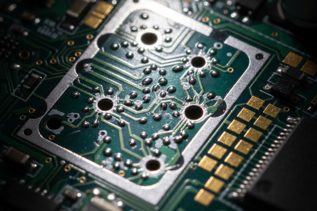
RF shields break this model. A shield is a metal enclosure soldered to the board to create an electromagnetic barrier. During reflow, this enclosure becomes a semi-sealed chamber, isolating the interior from the oven’s atmosphere. Any gases generated inside are trapped. This is fundamentally different from the open-board environment where most components live.
The trap is set by the interaction between this enclosed space and the board’s materials. Solder mask, an epoxy-based polymer, absorbs moisture from the air. When heated past its glass transition point, these trapped volatiles expand and seek release. On an open board, they simply vent into the oven. Under a shield, they are trapped. The tented vias, meant to be sealed barriers, now become weak points. The solder mask film over a via is thinner than the surrounding mask, and as pressure builds from outgassing, this thin film can rupture or blister. What emerges is not a clean release of vapor, but a localized defect that blasts through molten solder.
What Happens Under the Shield
The reflow process for lead-free solder typically peaks near 250°C, well above the 120-150°C glass transition temperature of most solder masks. As the board heats up, the mask’s epoxy transitions from a glassy, rigid state to a more rubbery one. This allows absorbed moisture to vaporize and migrate, creating internal pressure gradients that find their weakest point: the thin mask over a via.
The Outgassing Mechanism
Outgassing is the violent release of trapped gas from a material under heat. During the 30 to 90 seconds of peak reflow, the thin film of solder mask over a via—often only 15-25 microns thick—must contain this pressure. If the film ruptures, gas escapes rapidly into an environment where solder paste is fully molten.
This jet of escaping gas and epoxy decomposition products creates turbulence, propelling tiny droplets of solder away from their pads. These solder balls scatter across the interior of the shield enclosure, creating a minefield of potential defects.
How Solder Balls Form and Why They Matter
Solder balls are small spheres of alloy that form when molten solder is displaced and solidifies in isolation. The gas jet from a ruptured via launches these droplets, which naturally form spheres due to surface tension. As the board cools, they solidify wherever they land.
The electrical risk is straightforward. A conductive sphere can bridge two traces, creating a short circuit. Even if it doesn’t cause an immediate failure, a loose solder ball is a reliability time bomb; vibration or thermal cycling can dislodge it, causing a short later in the product’s life. For high-reliability applications in automotive, medical, or aerospace, the mere presence of solder balls is a criterion for rejection.
The mechanical risk is more subtle. Solder balls trapped under a shield can prevent it from seating flush against the board, degrading shielding effectiveness. In extreme cases, a ball lodged between the shield and a component can create mechanical stress, leading to component cracking or solder joint fatigue. Reworking a board to remove a shield is time-consuming and expensive, often requiring a full reflow cycle and risking damage to the board and the shield itself.
Via Treatments That Survive Reflow

The solution is to eliminate the thin solder mask film over the via and provide a controlled path for any outgassing. Three primary alternatives exist for vias under RF shields.
Open Vias: The simplest choice is to leave vias open, with no solder mask over the opening. This creates a clear vent path for any moisture or volatiles in the laminate, preventing pressure buildup. The main concern with open vias—solder wicking into the barrel—is rarely an issue under shields, as shield mounting pads are large and not typically adjacent to fine-pitch components. This is the lowest-cost and most direct solution.
Filled Vias: Here, the via barrel is filled with a non-conductive epoxy, then planarized and plated over. This eliminates the void space that traps moisture, effectively preventing outgassing from the via barrel. Filled vias are significantly more expensive and are typically reserved for via-in-pad designs where a component must sit directly over the via. While effective, this is often overkill for the area under a shield.
Plugged Vias: A middle ground, a plugged via is filled with a solder mask or resin plug that sits just below the surface. The plug prevents solder wicking but doesn’t create a hermetic seal. While less expensive than fully filled vias, they offer limited advantage over open vias in this specific application, as the primary goal is venting, not sealing.
A related and more cost-effective approach is via-near-pad. By placing open vias just outside the shield mounting pads—maintaining a clearance of at least 0.2 mm from the solder paste deposit—you get the necessary electrical connection without the risk of wicking or the cost of filling.
Designing for Rework
Avoiding tented vias is the first step. The next is designing for the reality that shields often need to be removed for debug, repair, or upgrades.
Solder mask openings around the shield perimeter should be sized to allow access for rework tools. A common practice is to define an opening that extends 0.1 to 0.15 mm beyond the shield pad. This provides a visual guide and ensures the entire solder joint is accessible. If the opening is too tight, the mask acts as a heat sink, making rework difficult; too large, and it exposes adjacent traces to potential damage.
Assume from the start that the shield will be removed. Design the mounting pads with enough thermal mass and solder mask clearance to survive multiple rework cycles without lifting. This means using pads larger than the minimum required for attachment and documenting the correct rework procedure, including tool temperature and dwell time.
Test Point Strategy When Shields Block Access
An RF shield is a wall, blocking direct probe access to the signals inside. Critical test points must be relocated outside the shield’s perimeter during the design phase.
For power and ground nets, this is simple, as they can be accessed elsewhere on the board. For sensitive RF or high-speed signals, the solution is often a small, AC-coupled probe pad located just outside the shield wall. This allows for testing without compromising shielding integrity, though the small parasitic capacitance must be accounted for in the design.
Distinguish between via stitching and test vias. The dense arrays of small vias under a shield are for grounding, not testing. If you need to probe a ground connection, add a dedicated, larger-diameter test via near the perimeter, clearly marked on the silkscreen.
Fixing an Existing Design
If you’re already facing outgassing issues on a board designed with tented vias, your options are limited. The best course is a Gerber-level revision, requesting the fabricator to remove the solder mask over the vias in the affected area. If boards are already built, pre-baking them at 120°C for several hours before assembly can drive out some moisture and reduce the severity of outgassing. However, neither of these process adjustments is a substitute for designing the board correctly from the start.
 Circuit Board Assembly")


