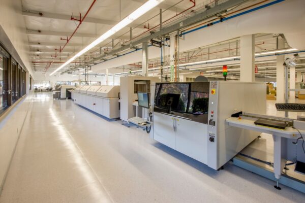
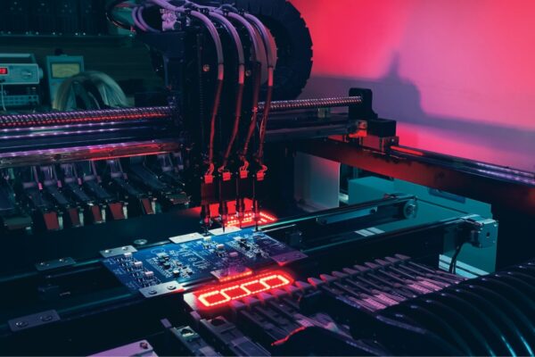
The sound of a heavy component dropping off a PCB inside a reflow oven is distinct. It’s not a loud crash; it’s a muffled, mechanical clunk that usually happens in Zone 6 or 7, right when the solder reaches its liquidus state. If you’re lucky, the part falls harmlessly onto the oven floor. If you’re unlucky—and the laws of probability suggest you will be—it lands on the conveyor mesh, jams the drive mechanism, or catches fire as it cooks in the peak zone for an hour.
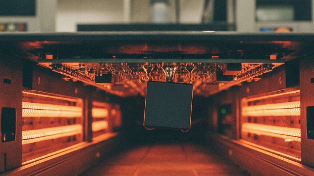
When you run a double-sided assembly, you’re effectively asking physics to look the other way for three minutes. The top side is easy; gravity helps hold the parts down. But when you flip that board over for the second pass, gravity becomes the enemy. The only thing keeping your expensive shielded power inductors and BGA packages attached to the board is the surface tension of molten solder. That’s a tenuous relationship. It works right up until the component’s mass overpowers the wetting force of the liquid metal. Then you have a line-down situation that no amount of process tweaking can fix.
The Physics of the Wetting Force
To understand why parts stay on—and exactly when they won’t—look at the battle between mass and surface tension. When the solder paste reflows on the second side, it liquefies. For a standard SAC305 alloy, the surface tension is surprisingly high, roughly 500 dynes/cm. This force acts like a microscopic spring, pulling the component toward the center of the pad. For the vast majority of components, this force is orders of magnitude stronger than gravity. An 0201 capacitor or a standard SOIC package isn’t going anywhere. They are so light relative to their pad area that they could ride through the oven upside down, sideways, or vibrating violently, and they would still self-align.
That safety margin evaporates as components get heavier and their termination areas stay relatively small. Engineers often assume that if a part has a large footprint, it has a large solderable area. This is false. A shielded power inductor might be a massive 12mm x 12mm block of ferrite and copper weighing 1.5 grams, but it might only anchor to two relatively small pads. You need to check the Cg/Pa ratio—the Gravitational Force (Cg) versus the Total Pad Area (Pa).
There is a persistent “hack” in prototype shops where engineers suggest using Kapton tape to hold these parts in place. For a run of five boards, you might get away with it, provided the tape doesn’t leave residue or outgas and contaminate the joint. For production, it’s a liability. Tape fails, adhesive cooks, and it adds a manual removal step that risks ripping the component off the board entirely.
The industry rule of thumb is often cited around 30 grams per square inch of solderable pad area. If the component load exceeds this, surface tension won’t hold it against gravity. But this is a static calculation. It doesn’t account for the vibration of a worn-out chain conveyor or the high-velocity air convection in a Heller MKIII oven. If your calculation says you are at 90% of the limit, you’re actually at 110% of the risk limit once real-world dynamics apply. If the math is borderline, the part will fall.
Design: The Only Free Solution
The most effective way to keep heavy parts from falling off the bottom side is to never put them there in the first place. It sounds obvious, yet board layouts frequently arrive at the factory floor with massive connectors, heavy transformers, and large BGAs placed on the secondary side simply because “they fit.”
This is often a failure of visualization. In the CAD tool, the board is a flat, abstract logic puzzle. In the factory, it’s a physical object subjected to thermal stress. A 10mm electrolytic capacitor on the bottom side is a ticking time bomb. If the layout engineer moves that capacitor to the top, the problem vanishes for zero dollars. If they leave it on the bottom, you are committed to a lifetime of glue dispensing or fixture purchases.
Sometimes, density constraints make this impossible. You can’t fit everything on the top side of a modern smartphone or a high-density ECU. But there is a hierarchy of placement. Low-mass passives go on the bottom. Low-profile QFNs go on the bottom. Heavy, tall, or shielded components must fight for space on the top. If a heavy part must be on the bottom, the designer should increase the pad size to maximize the wetting area, giving the solder more surface tension to grip—though even that has limits before you start seeing tombstoning issues.
The Glue Delusion

When design changes are rejected, the conversation inevitably turns to glue. “Just glue it,” says the project manager, imagining a simple dab of adhesive that solves the problem. In reality, introducing SMT adhesive (usually a red epoxy) is a desperate move that trades a mechanical problem for a chemical and process nightmare.
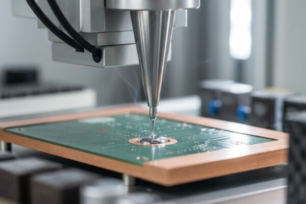
Dispensing glue isn’t free. It requires a dedicated machine or a dedicated step in the pick-and-place cycle. You need a jet valve or a stencil printer to apply the dots. If you use a stencil, you now have a stepped stencil requirement—one thickness for paste, another for glue—which is complex to print reliably. If you use a dispenser, you’re adding cycle time. A dispenser like an Asymtek is precise, but nozzles clog. The epoxy has a shelf life. If the dot is too tall, it smears; if it’s too short, it doesn’t touch the component body.
Then there is the rework. SMT adhesives are thermosetting epoxies designed to withstand reflow temperatures of 240°C+. They cure hard. If that glued inductor fails a functional test, you cannot simply desolder it. You have to mechanically break the bond. This often means prying the component off, which frequently rips the copper pads right off the FR4 laminate. You haven’t just lost the component; you’ve scrapped the board.
There is also confusion about what glue to use. People search forums for “high temp super glue,” but consumer adhesives outgas and fail instantly in a reflow oven. You must use industry-standard SMT epoxies (like Loctite 3621), and they must be cured. The curing profile for the glue might conflict with the reflow profile of the solder paste, forcing you to compromise the metallurgical bond just to set the adhesive. It is a path filled with hidden costs.
The Pallet Reality (and Tax)
If the layout is frozen and glue is too risky, the professional solution is a selective reflow pallet (or fixture). This is a carrier, usually machined from a composite material like Durostone or Ricocel, that holds the PCB. It has pockets routed out to shield the bottom-side components, protecting them from the air flow and keeping them from dropping if the solder reflows.
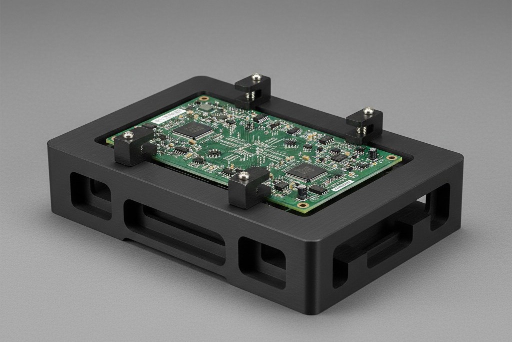
This solves the retention problem instantly. The heavy parts on the bottom are physically supported or shielded so they never reach reflow temperatures again. However, pallets introduce a massive “thermal tax.” You are introducing a heavy slab of composite material into the oven. This material absorbs heat.
A pallet can weigh a kilogram or more. When you run your thermal profile, you will see a massive heat sink effect. The parts sitting on top of the thick pallet rails might not reach the required peak temperature of 235°C–245°C. You might solve the dropping inductor problem only to create “Head-in-Pillow” defects on your top-side BGA because the balls didn’t fully collapse. To fix this, you have to crank up the oven temperatures or slow down the conveyor speed to let the heat soak in. This reduces your throughput (units per hour) and risks overheating sensitive components that aren’t shielded by the pallet.
And then there is the sticker shock. A good selective reflow pallet costs between $300 and $800. You don’t need one; you need 50 or 100 to fill the oven loop. Suddenly, keeping that heavy inductor on the bottom side costs $30,000 in tooling before you’ve sold a single unit.
The Decision Path
Gravity is consistent. It does not care about your project timeline or your budget constraints. When you are staring at a BOM with heavy bottom-side parts, you have three choices, and you must make them in this order:
- Audit the Design: Fight to move the heavy parts to the top. Use the Cg/Pa ratio to prove to the design team that the part will fall. Show them the math.
- Buy the Pallets: If the design is frozen, budget for fixtures. Accept the cycle time hit and the thermal profiling complexity. It is the only robust way to run volume production for heavy bottom-side parts.
- Glue as a Last Resort: Only if you cannot use pallets (due to clearance or budget) and cannot change the design should you look at dispensing epoxy. Understand that you are increasing your scrap rate and rework difficulty permanently.
Do not trust hope. Do not trust that “it held on the prototype.” Trust the mass of the part, the area of the pad, and the unyielding force of gravity.
