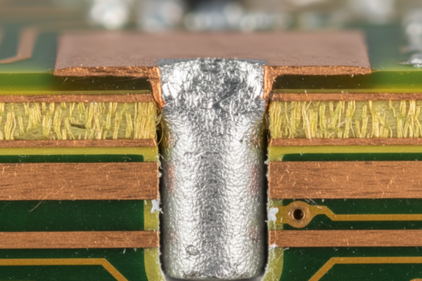
Selective soldering is often treated as a process control problem. When bridges appear between adjacent pins, the first impulse is to adjust dwell time, tweak flux, or lower the solder pot temperature. While these variables matter, they operate within constraints set much earlier: the geometry of the through-hole itself. If a hole is designed incorrectly, no amount of process optimization will reliably prevent bridges. The solder will find a path between pads because the physical design makes that path inevitable.
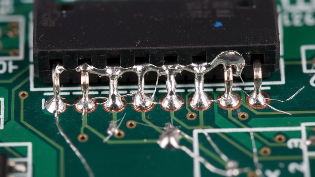
We see this pattern constantly. A board with a high-pin-count connector arrives for selective soldering, and bridges form on every run despite competent process engineering. The root cause isn’t the machine or the operator. It’s a finished hole size with 0.08mm of clearance instead of 0.20mm, a thermal relief with spokes aimed directly at an adjacent pad, or a keepout violation that forces the nozzle into a compromised angle. These are design decisions, and they determine whether a board sails through production or gets trapped in rework.
This article explains why. We will explore the physics of bridge formation and derive the hole geometry rules that prevent them, focusing on the design choices that truly matter: lead-to-hole clearance, thermal relief orientation, nozzle access, and strategies for high-thermal-mass components. These aren’t arbitrary guidelines; they are the mechanical and thermal realities of how solder behaves in a barrel.
Why Selective Solder Bridges Form
A solder bridge isn’t a random defect. It is the predictable result of solder establishing a continuous path between two points that must remain isolated. In selective soldering, this happens when the solder in two adjacent through-hole barrels makes contact, either on the board’s top surface or within the barrels themselves.
The Role of Capillary Action
When a nozzle applies molten solder to a through-hole, the solder doesn’t just pool on the surface. It rises through the barrel via capillary action, pulled upward against gravity by the surface tension and wetting forces between the solder and the copper barrel wall.
The height of this capillary rise depends on the annular gap between the component lead and the barrel. A narrow gap creates a strong capillary force, pulling solder high and fast. A wide gap creates a weaker force, and the solder may stall, leaving a void. The problem is that the barrel isn’t an open tube; it contains a lead. If the clearance is too small, the barrel fills with more solder than the joint requires. That excess has nowhere to go but out, spreading across the top-side pad.
This overflow forms a meniscus at the pad’s edge. If two adjacent pads both have excess solder, their menisci touch. In that instant, surface tension pulls the two pools into a single mass. A bridge is formed.
When Adjacent Barrels Become One
The critical variable is pitch—the center-to-center distance between leads. At a standard 2.54mm pitch with proper hole clearance, there is enough space between pads to keep menisci apart. At 1.27mm pitch with improper clearance, that margin for error vanishes.
The interaction is both geometric and thermal. Two adjacent pads on a shared plane create a continuous copper path that conducts heat. If a nozzle dwells on one pad and immediately moves to the next, the first pad is still molten. Solder from the second pad can wick toward the first through the copper, especially if thermal reliefs are missing or poorly oriented.
Bridges form because the boundary conditions permit them. The solder is simply obeying physics, minimizing its surface energy by forming the smallest possible surface area. For two close, overfilled pads, that means a single shared mass. Instead of fighting this behavior with process tricks, the solution is to design boundary conditions that prevent it from happening in the first place.
Lead-to-Hole Clearance That Prevents Bridges
The single most critical design parameter for selective soldering is the diametral clearance between the component lead and the finished hole. This gap dictates the volume of solder entering the barrel, the strength of the capillary rise, and whether excess solder overflows onto the top surface. Get this wrong, and bridges are almost guaranteed.
The Ideal Clearance: 0.15mm to 0.25mm
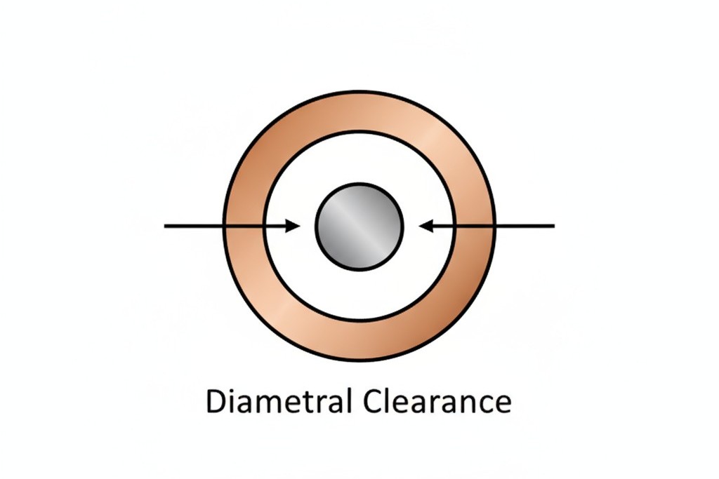
For selective soldering, the functional range for diametral clearance is a tight window: 0.15mm to 0.25mm. This is much tighter than the typical range for wave soldering, which can tolerate 0.40mm or more. The difference lies in the application method. A wave floods barrels from below with high kinetic energy, while a selective nozzle applies solder locally with far less force. The barrel itself must do more of the work to draw the solder upward.
- Below 0.15mm: The barrel is too tight. The narrow annular gap creates an overpowering capillary force that pulls too much solder into the joint. The barrel overfills, solder spreads across the top-side pad, and bridging becomes likely.
- Above 0.25mm: The barrel is too loose. The capillary force weakens, and solder may not rise fully to the top, leaving a void or a cold joint. This is unacceptable for high-reliability applications.
The 0.15mm to 0.25mm range is the sweet spot where capillary action is strong enough to fill the barrel reliably but not so strong that it overfills. The solder wets the pad and lead to form a controlled fillet without spreading beyond the pad boundary.
Calculating Finished Hole Size
The finished hole is the diameter after plating, not the drill size. To calculate it, start with the maximum lead diameter from the component datasheet and add your desired clearance (typically 0.20mm as a nominal target). This is your finished hole diameter.
To find the drill size, subtract twice the plating thickness. For a standard board with 25 microns (0.025mm) of copper plating in the barrel, you subtract 0.05mm. For example, a 0.64mm square pin has a diagonal of roughly 0.90mm. For a 0.20mm clearance, it needs a 1.10mm finished hole, which requires a 1.05mm drill.
This level of precision requires coordination with your fabricator to ensure plating thickness is controlled and the finished hole size is verified. It also demands that you know the component lead diameter accurately. While general guidance like IPC-7251 exists, it is written for wave soldering and prioritizes ease of insertion. For selective soldering, solder volume control is paramount. The tolerances must be tighter and they must be defended.
Thermal Reliefs and Solder Flow Control
Thermal reliefs are known for reducing the heat-sinking effect of a plane, but their role in selective soldering is more complex. They also control the direction and symmetry of solder flow. The spokes of a thermal relief are preferential paths for both heat and molten solder. Their design determines whether solder flows evenly or concentrates in a direction that creates a bridge.
Spoke Count and Width
A four-spoke relief distributes heat more evenly than a two-spoke design, but if the spokes are too wide, they can act as channels for solder to wick outward. A spoke width of 0.30mm or less provides good thermal isolation without creating a significant solder flow path. At 0.50mm or more, a spoke begins to act like an extension of the pad itself. For high-current applications demanding wide spokes, their orientation becomes critical.
In some high-power designs, thermal reliefs can’t be used at all. For these direct plane connections, hole clearance becomes even more crucial, and the process must compensate with extended preheat. The bridging risk is higher because the pad is thermally tied to its neighbors, creating a continuous hot zone.
Orientation to Minimize Bridge Paths
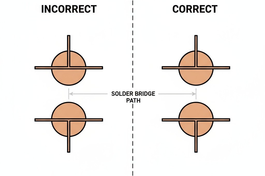
If two adjacent pads have two-spoke reliefs oriented directly toward each other, you have created a thermal and fluidic highway for a bridge. Heat and solder will flow along the spokes, meeting in the space between the pads.
The solution is simple: rotate the reliefs.
- For a two-spoke relief, orient the spokes perpendicular to the row of pins.
- For a four-spoke relief, orient the spokes at 45 degrees to the pin row.
This ensures no spoke points directly at an adjacent pad, creating a more symmetric thermal environment. On a 1.27mm pitch connector, rotating misaligned reliefs by 90 degrees can eliminate bridging without changing any other variable.
Keepout Rules for Nozzle and Pallet Access
Selective soldering is a physical process. A nozzle must position itself under the board and a pallet must hold that board without obstructing the nozzle’s path. If the layout ignores these spatial requirements, the process fails before it even begins.
Horizontal Clearance for the Nozzle
A solder nozzle has a physical diameter, typically 4mm to 8mm. It needs radial clearance around the target pad to avoid colliding with adjacent components. As a rule of thumb, a 6mm nozzle requires a keepout radius of about 5mm from the center of the pad to the edge of any nearby component.
This is a larger footprint than many designers expect, especially on dense boards. While most machines allow the nozzle to approach at an angle to reduce this requirement, an angled approach creates asymmetric heating and may require longer dwell times. Sufficient clearance for a vertical approach is always preferred. Connectors at the board edge are a common challenge, as the nozzle cannot extend beyond the board boundary. This constraint must be recognized during layout, not discovered during process development.
Vertical Clearance and Component Height
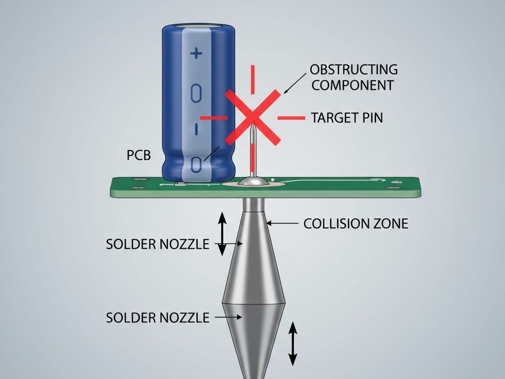
The nozzle must also rise from below the board to wet the joint. A tall component next to the target pad can physically block the nozzle. This Z-axis clearance problem requires a vertical keepout zone. Components taller than the nozzle’s working height should not be placed within the horizontal clearance radius of selective solder joints. This is a 3D design problem that requires coordination between mechanical, layout, and process engineering, often checked manually or with custom design rule scripts.
Design Strategies for High-Mass Connectors
High-pin-count connectors are a perfect application for selective soldering, as they often can’t survive reflow. They are also the most difficult to solder due to their high thermal mass. The large metal shell and dense pin array act as a massive heat sink, pulling energy away from the joint faster than the nozzle can supply it.
Why Thermal Mass Prevents Good Wetting
A connector with high thermal mass absorbs a huge amount of energy. During soldering, the nozzle applies heat locally, but that heat is immediately conducted into the connector body and any connected copper planes. The solder never reaches its ideal wetting temperature, or does so only briefly. The result is a cold joint or a partial fill. A common process mistake is to compensate by extending the dwell time, which applies so much solder that it overflows and creates bridges.
The design solution is to thermally isolate the joint as much as possible. This means using thermal reliefs with the thinnest spokes that can still carry the required current. Another option is a localized cutout in a plane beneath the connector, just large enough to break the thermal connection during soldering while maintaining overall plane integrity.
Pin Stub Length and Solder Volume
The length of the pin stub extending above the board’s top surface also affects the solder volume. A long stub increases the total length of the barrel that must be filled. If hole clearance is already tight, a long stub can easily cause an overflow.
For selective soldering, the stub should be trimmed to the minimum length needed for inspection, typically 0.50mm to 1.50mm. Longer stubs add no value to joint strength and only increase the risk of defects. If a component is supplied with long leads, they should be trimmed before or after insertion. The cost of this extra step is trivial compared to the cost of reworking bridges on a hundred-pin connector.
Designing for Process Latitude
The rules in this article are not preferences; they are the physical requirements for a reliable selective soldering process. A board designed with 0.20mm lead-to-hole clearance, properly oriented thermal reliefs, and adequate nozzle keepouts will solder cleanly with minimal tuning. A board that ignores these fundamentals will struggle, no matter how skilled the process engineer.
The goal of design-for-manufacturability is to create margin, allowing for slight variations in the process or components without causing failures. Tight clearances and poor thermal design eliminate that margin, demanding a level of perfection that is not a sustainable manufacturing strategy.
These critical decisions are made during layout, often without a full understanding of their downstream consequences. A pre-production design review can catch a keepout violation or an undersized hole when the fix is a simple CAD revision. After fabrication, the fix is a new board spin or a costly, unreliable process workaround.
To make selective soldering work, the checklist is short but non-negotiable. Ensure lead-to-hole clearance is between 0.15mm and 0.25mm. Orient thermal reliefs away from adjacent pads. Provide at least 5mm of radial clearance for the nozzle. Isolate high-mass connectors thermally. And keep pin stubs under 1.50mm. These are the rules that separate a successful product from a production nightmare.
