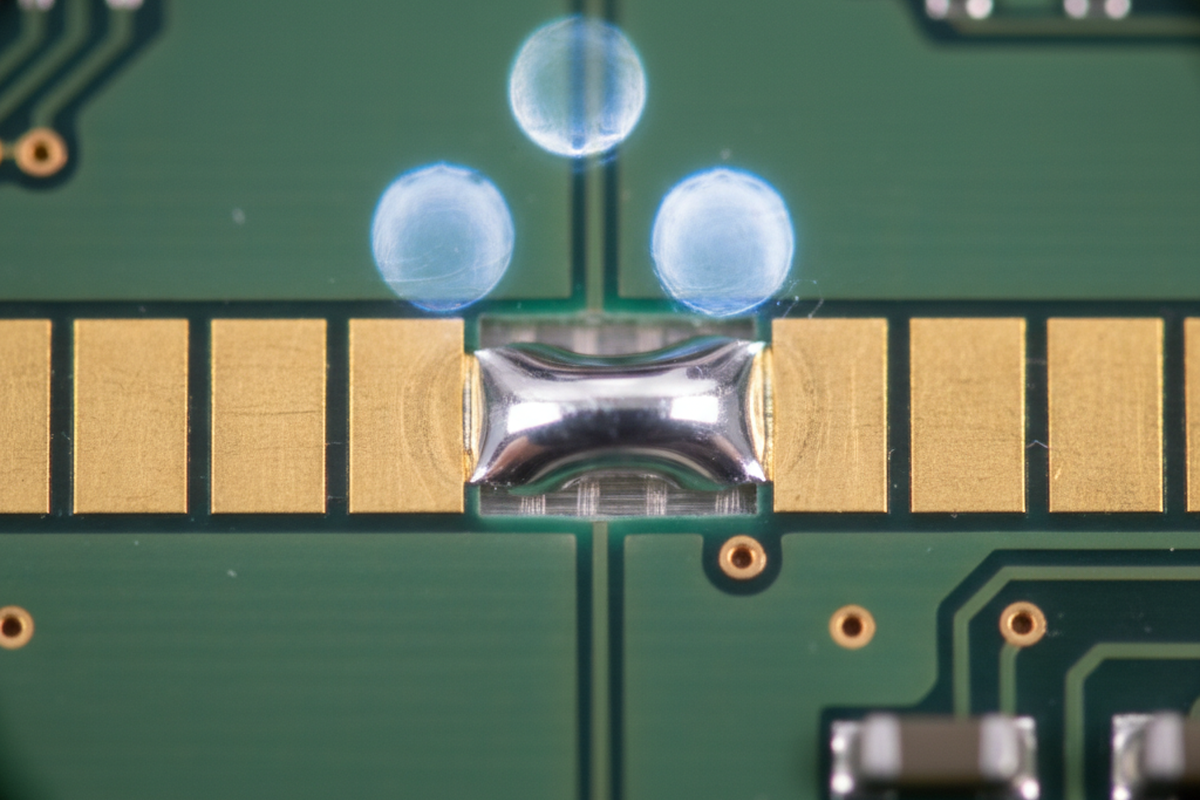
The smell of a bad solder mask decision is distinct. It smells like burnt flux, hot polyimide, and a Saturday afternoon spent hunched over a Mantis microscope with a soldering iron in hand. When you look at a QFN-32 under 10x magnification and see every single pin bridged to its neighbor, you aren’t thinking about elegant routing or signal integrity simulations. You are looking at a physical failure of containment. The solder paste, once heated in the reflow oven, had nowhere to stop. It slumped, wicked, and merged because the mechanical dam supposed to separate pad 1 from pad 2 simply wasn’t there.

Don’t blame the soldering iron, and stop blaming the stencil. This is a data issue that became a physical nightmare. The root cause sits in the CAD settings, often left at a “safe” default of 4 mils expansion, which quietly deletes the solder mask web between fine-pitch pads. Physics does not care about your render. If the dam is missing, the solder will bridge.
Why The Fab House Wants to Ruin Your Assembly
Your bare board fabricator and your assembler have a fundamental conflict of interest. The fabrication house is terrified of “encroachment.” If they print the green mask layer slightly off-target (a guaranteed reality of wet-film processing) and that mask lands on top of a copper pad, you will reject the board for poor solderability. To protect themselves from scrap costs, they demand a safety buffer. They want you to expand the mask opening so that even if their alignment drifts by 2 or 3 mils, the opening still clears the pad.
This safety margin saves them money, but it costs you reliability. When you apply a global expansion rule—say, the industry standard 4 mils (0.1mm)—to a 0.5mm pitch component, you mathematically eliminate the bridge between the pads. You are trading a potential cosmetic defect (mask on pad) for a guaranteed functional defect (solder bridging).
If you deal with budget fabrication shops, you will often get the dreaded “Engineering Query” or “On Hold” email. They will flag your fine-pitch footprints and claim the “sliver” of mask between pads is too thin to print reliably. They aren’t lying; their process might not be able to hold a 3-mil web without it flaking off. But if you let them “fix” it by removing the web entirely, you authorize them to create a lake of exposed copper where there should be discrete islands. They prioritize their yield over yours.
The Mechanics of the Dam
Solder mask functions less like paint and more like a hydraulic dam. Its primary job in a reflow oven is to break the surface tension of molten solder. When paste melts, it wants to minimize its surface area. If a strip of mask material sits between two pads, the solder beads up on its respective pad, contained by the mask wall. This is the “gasket” effect. The mask provides a vertical wall for the stencil to sit on, and a horizontal barrier the solder cannot wet to.
When you remove that dam—either through aggressive expansion settings or a fab house engaging in “gang relief”—you lose containment. The space between the pads becomes bare FR4 laminate. Molten solder easily wicks across that gap, especially if the stencil aperture was designed assuming a gasket seal. Without the mask height to block it, the solder slumps.
This is often where the panic sets in for BGA components. You might see shorts under X-ray and assume the paste volume is too high or the profile is too hot. Look at the bare board first. If the mask openings for the BGA pads are so large that they touch, you have created a path of least resistance for the solder ball to merge with its neighbor. Non-Solder Mask Defined (NSMD) pads are standard for BGAs to improve reliability, but if the expansion is too aggressive, the “moat” around the pad becomes a channel for bridging.
The Gang Relief Trap
The most dangerous version of this problem hits QFNs and fine-pitch connectors. Designers, tired of fighting DRC (Design Rule Check) errors about “minimum solder mask sliver,” often take the path of least resistance: Gang Relief. This involves drawing a single large rectangle of mask opening over an entire row of pins.
It looks clean in the Gerber viewer. It passes the fab house checks immediately because there are no delicate slivers to print. But on the assembly line, it is a disaster. I have seen trays of expensive silicon—QFP-100s on medical device prototypes—scrapped because of this. When you gang relieve a row of 0.5mm pitch pins, you are asking the surface tension of the solder to be the only thing keeping the joints separate. It rarely works. The solder pulls together, and you end up with a single bar of alloy shorting out ten pins.
Manual rework on these is brutal. You have to wick away all the solder, clean the area with alcohol, and try to drag-solder fresh joints without a mask dam to guide you. It turns a $5 board assembly into a $50 rework project.
The LDI Threshold

You can’t just keep shrinking the web; eventually, the material physically fails. The real solution is paying for precision. Traditional photo-imageable processes need that slop factor. Laser Direct Imaging (LDI) changes the math. LDI doesn’t use a film. It uses a laser to cure the mask directly on the board, referencing the board’s own fiducials for alignment.
With LDI, you don’t need 3 or 4 mils of expansion. You can run 1:1 mask (zero expansion) or a very tight 1-mil expansion. This allows you to keep a robust 3-mil dam even on 0.4mm pitch parts. Yes, LDI costs more. It is a premium process. But weigh that cost against the cost of rework. If you are building a consumer gadget with 0805 passives and SOIC chips, save your money and use the sloppy process. But if you are putting down 0.4mm pitch QFNs or 0.5mm BGAs, the “savings” on the bare board will evaporate the moment the first bridge is detected at AOI.
The New Baseline
Stop trusting the defaults in your EDA tools. A global expansion of 4 mils is a relic from a time when components were huge.
For any component with a pitch of 0.5mm or less, you must intervene:
- Check the Web: Ensure there is at least 3 mils (0.075mm) of mask between the pads in your design.
- Audit the Expansion: If maintaining that web requires reducing expansion to 0 or 1 mil, do it.
- Specify LDI: If you tighten the expansion, tell the fab house you require LDI. If you don’t, they will put you on hold or, worse, just expand it back without telling you.
- No Gang Relief: Never allow a row of pins to share a single mask opening unless the datasheet explicitly demands it (which is rare).
The mask is part of the mechanical assembly. Treat it with the same precision you treat the copper.


")

