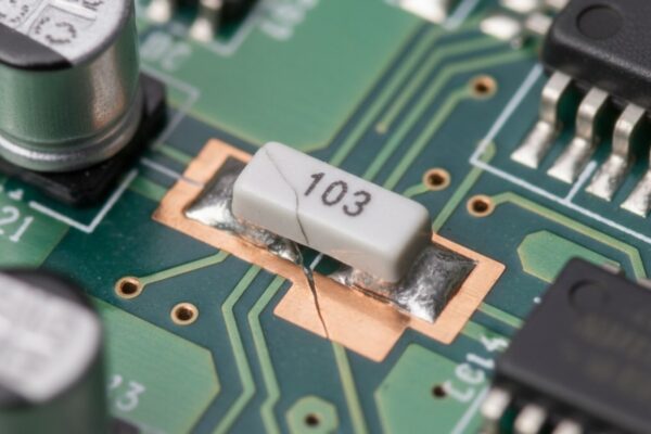
The solder joints beneath a ball grid array package are invisible to the naked eye and to conventional optical inspection. For micro-BGA and chip-scale designs, where hundreds of connections hide under a component no larger than a fingernail, this inaccessibility is a serious verification problem. A defective joint can pass visual checks, survive basic electrical tests, and still fail catastrophically in the field when thermal cycling or vibration reveals a latent weakness. The question isn’t if these hidden joints can fail, but how to find the bad ones before a product ships.
At Bester PCBA, we address this with a dual verification methodology: automated X-ray inspection (AXI) to assess the structural quality of every solder ball, followed by on-bench power cycling to validate performance under stress. Neither method alone is enough. AXI reveals voids, wetting defects, and alignment errors that signal poor process control, but it cannot detect a joint that looks good while having poor conductivity. Power cycling proves that the joint not only has the right structure but behaves correctly under real-world electrical and thermal loads. Together, they form a strategy that slashes the risk of hidden defects reaching customers.
This isn’t a theoretical exercise. The physics of modern packages and the brutal economics of field failures demand a rigorous approach. Understanding why each method matters, what it reveals, and how they complement one another is essential for anyone designing or sourcing assemblies with dense area-array packages.
Why Hidden Solder Joints Demand Specialized Verification
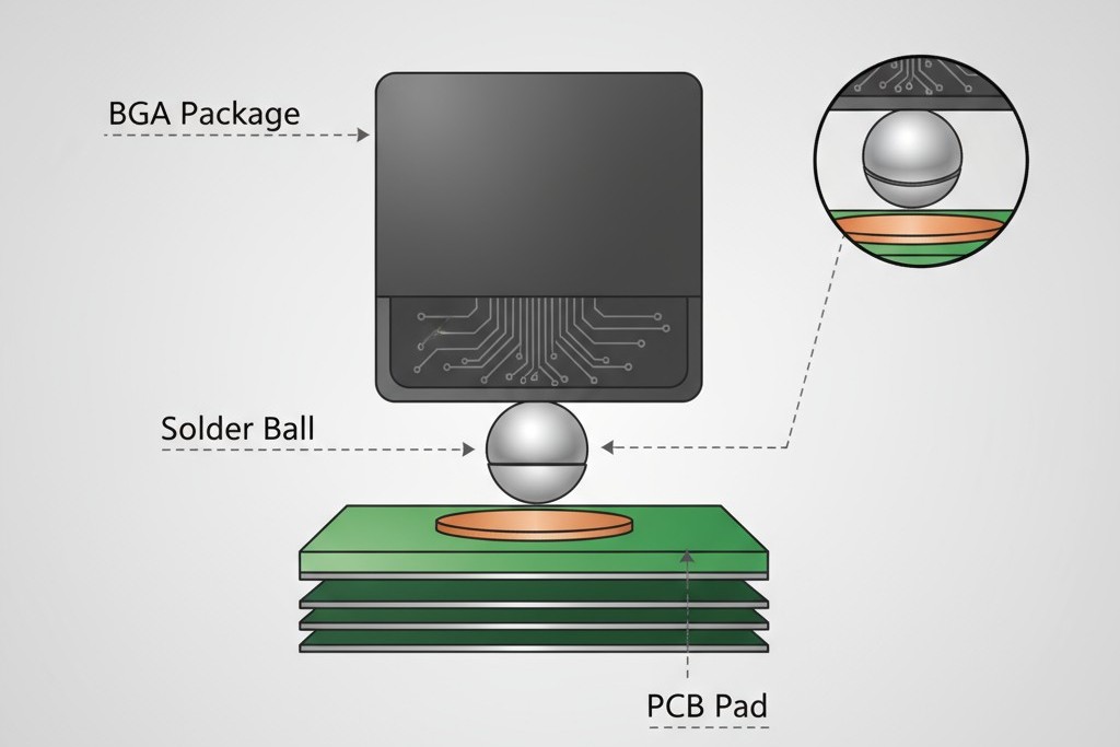
A ball grid array (BGA) component connects to a board through an array of solder balls on its underside, not through leads extending from its body. During reflow, these balls collapse and wet to matching pads on the board, forming joints completely obscured by the package. This design offers huge advantages in density and electrical performance, enabling fine-pitch connections and short signal paths. It also eliminates the direct inspectability of a traditional leaded component.
Optical inspection systems, manual or automated, rely on reflected light to judge solder fillet shape and joint formation. For a BGA, there is no fillet to see. The package body blocks any line of sight to the joint. An automated optical system can verify component presence and placement, but it cannot see the solder connection itself. The only external clue—the standoff height of the package—offers a crude guess at solder volume but reveals nothing about internal voids, non-wetting, or bridging.
This challenge intensifies as density increases. A 0.5 mm pitch micro-BGA with 256 balls presents 256 opportunities for a defect that optical methods will miss. Chip-scale packages, where the die is nearly the same size as the package, push this further with even finer pitches. The margin for error shrinks, and relying on process control alone becomes a gamble. For high-reliability assemblies, that gamble is unacceptable.
The industry’s response was to find a way to see through the package. Automated X-ray inspection is the dominant solution, but it addresses only half of the verification problem. Understanding its capabilities, and its limits, is the first step toward a complete strategy.
The Structural Inspection: What AXI Reveals in BGA Arrays
How X-Ray Imaging Penetrates the Package
X-rays occupy a region of the electromagnetic spectrum with wavelengths far shorter than visible light. At these wavelengths, photons carry enough energy to penetrate materials opaque to our eyes, including the epoxy or ceramic body of a BGA package. The degree of penetration depends on material density. Metals used in solder, like tin-lead or tin-silver-copper alloys, have high atomic numbers and absorb X-rays more strongly than the lighter elements in the board or package. This differential absorption creates contrast.
An AXI system directs an X-ray beam through the assembly, and a detector on the opposite side captures the transmitted radiation. This forms a shadow image where denser materials appear darker. The solder balls under a BGA cast distinct shadows, making the gaps between them, voids within them, and the solder-to-pad boundary visible. The image is a density map, and interpreting it means understanding which structural features correlate with a reliable connection.
Modern AXI systems offer multiple viewing angles and tomographic reconstruction, allowing inspection of individual layers within a joint. This is critical for distinguishing between a harmless void at the package-side interface and a dangerous one at the board-side interface that compromises the thermal and electrical path. While the physics of imaging imposes limits—spatial resolution is finite, and microscopic cracks may go undetected—the method is unmatched for revealing the internal structure of a hidden joint.
The AXI Criteria for Acceptable Solder Joints
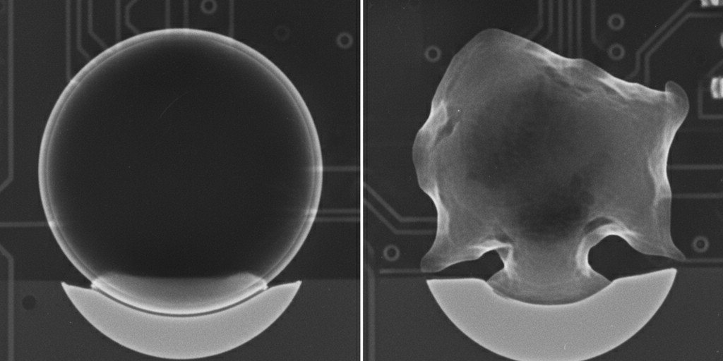
An X-ray of a BGA joint reveals a trio of structural tells. The most critical is complete wetting: the solder must have flowed and adhered to both the package and board pads, forming a continuous metallic bond. A properly wetted joint appears as a smooth transition from solder ball to pad. Any sharp gaps or regions of low contrast indicate non-wetting, a catastrophic defect that leaves the joint with no mechanical or electrical integrity.
Next, the joint must be centered and aligned. The solder ball should be centered over its pad, creating a symmetrical connection. Misalignment, often from placement error, reduces the effective contact area and increases stress concentration. AXI software measures this offset and flags joints that exceed a defined threshold.
Finally, AXI exposes voiding—gas pockets trapped within the solder during reflow, typically from outgassing flux or moisture. A void appears as a dark region inside the brighter solder ball. While small voids are nearly inevitable, their size, number, and location determine whether they compromise the joint.
Voiding Thresholds and What They Mean for Reliability
The link between void content and long-term reliability is not a simple one; it’s dictated by the joint’s function. For an electrical connection, a void shrinks the cross-sectional area and increases resistance. For a thermal path under a power device, it impedes heat transfer. For mechanical integrity, a large void can become a crack initiation site under thermal stress.
Industry standards vary, but a common baseline considers a total void area under 25% of the ball’s cross-section acceptable for most applications. Void content between 25% and 50% enters a conditional zone, where acceptability depends on the joint’s function; a low-power signal ball might pass, while a thermal ball would not. Anything exceeding 50% is typically rejected outright, as the joint’s ability to conduct current and dissipate heat is severely degraded.
Bester PCBA uses these thresholds as a starting point, adjusting them for specific designs. A high-reliability aerospace assembly may demand a strict 15% limit, while a consumer product might tolerate the standard 25%. Crucially, this threshold isn’t arbitrary. It’s derived from empirical data that correlates void content with field failures and thermal performance.
The distribution of voids also matters. A single void occupying 20% of the joint area is generally less concerning than five voids of 4% each, as the latter fragments the current path and creates multiple stress concentrations. AXI software can analyze these patterns, but the analysis is only as good as the programmed thresholds.
The Limits of Structural Inspection Alone
AXI is a powerful tool for assessing the physical formation of a solder joint, but it is fundamentally a structural inspection method. It measures geometry and density, not electrical resistance or thermal conductivity. This distinction is critical. A joint can look perfect on an X-ray and still be functionally useless.
Consider a cold solder joint. Insufficient heat may have resulted in a weak, high-resistance connection. The solder may have wet the surfaces with acceptable voiding, but the interface lacks a true metallurgical bond. An X-ray image of this joint looks normal. The defect is microscopic, in the quality of the intermetallic bond, and AXI cannot see it.
Similarly, a joint might pass AXI but have an intermittent connection that only appears under thermal stress. The joint works during initial testing, but as it heats up during operation, micro-movements break and re-establish contact. This failure mode is particularly insidious and difficult to diagnose. An X-ray is a snapshot at room temperature; it cannot predict how a joint will behave over time.
These limitations don’t diminish AXI’s value; they define its role. AXI verifies that the soldering process produced joints with an acceptable structure, free from gross defects. It is a necessary check, but it is not sufficient. To prove the joints will perform reliably, a functional test is required.
The Functional Validation: Power Cycling on the Bench
How Thermal and Electrical Stress Reveals Latent Defects
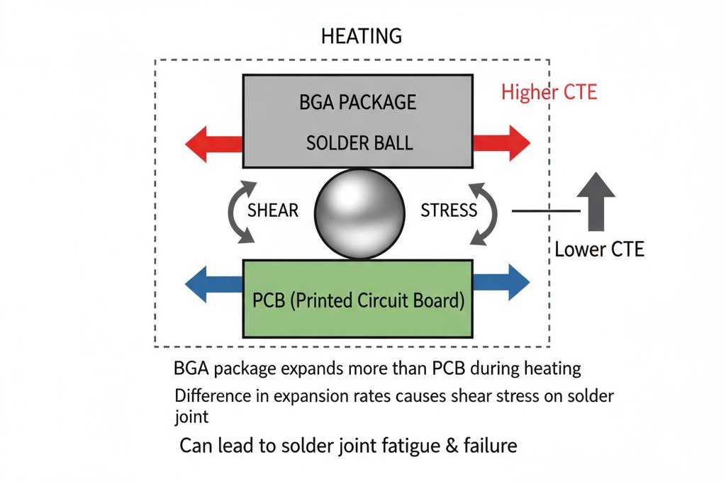
Power cycling subjects an assembly to repeated transitions between on and off states. When powered, current flows through the BGA joints, generating heat. This heating causes the solder, package, and board to expand at different rates, because their coefficients of thermal expansion are different. This mismatch creates mechanical stress at the solder joint interface. When power is removed, they cool and contract, reversing the stress.
A healthy joint with a strong metallurgical bond accommodates this stress. A weak joint with high resistance or a poorly formed intermetallic layer experiences localized heating and stress concentration. Over multiple cycles, micro-cracks form and propagate, resistance climbs, and the joint eventually fails. Power cycling accelerates this failure mechanism in a controlled lab environment. A joint that would fail after 500 cycles in the field might fail after 50 cycles on the bench, where temperature swings can be more aggressive. This is distinct from passive thermal cycling, which tests fatigue by changing ambient temperature but misses failures caused by the internal heating of a live circuit. Power cycling imposes both thermal and electrical stress at once, making it a more comprehensive functional test.
The Power Cycling Protocol for BGA Verification
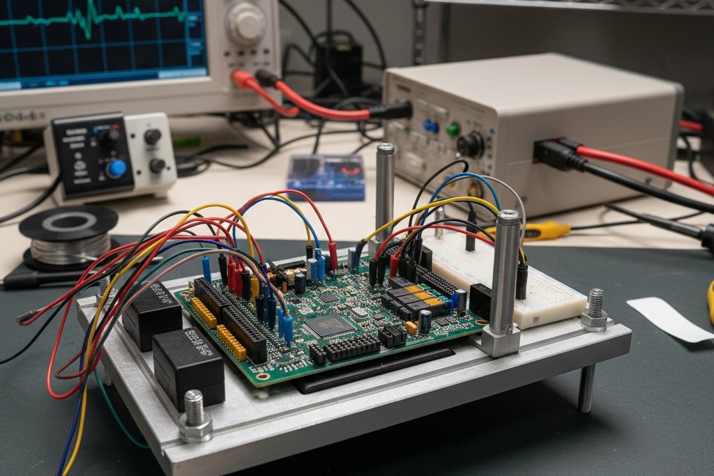
At Bester PCBA, the power cycling protocol is tailored to the device, but the framework is consistent. The assembly is placed in a fixture, and the device is powered to its nominal operating condition for a set dwell time, allowing it to reach thermal equilibrium. Power is then removed, and the board cools to a baseline temperature. This completes one cycle.
The number of cycles depends on the goal. A rapid screening of 10 to 20 cycles can catch gross defects like cold joints. A more rigorous validation of 50 to 100 cycles provides higher confidence. High-reliability applications may require several hundred cycles, approaching an accelerated life test.
Throughout the test, the assembly is monitored for functional failures. This can be as simple as checking if the device still works or as detailed as measuring supply current, output voltage, and signal integrity. A sudden current spike may indicate a short; a loss of function points to an open. Thermal imaging can also identify joints that run hotter than expected, flagging high resistance or poor heat dissipation. This data provides invaluable feedback on process margins, helping not just to catch defects but to understand how close the process is to a failure threshold.
Why the Dual Approach Delivers Confidence
AXI and power cycling serve complementary roles. AXI provides a rapid, non-destructive structural assessment of every single joint, catching defects from process variation before the board is ever powered on. Power cycling then validates that the joints AXI deemed structurally sound actually perform under the stresses of real-world operation.
The result is more than just additive. An assembly that passes both AXI and power cycling has demonstrated both structural integrity and functional robustness. While no test eliminates all risk, the confidence this dual approach provides is substantially higher than what either method could achieve alone.
For designs with micro-BGA or CSP components, where a single joint failure can be catastrophic, this dual approach is a best practice. At Bester PCBA, we apply both methods as a standard procedure for dense area-array assemblies, tailoring the thresholds and protocols to meet the application’s reliability demands. The investment in verification is justified by the reduction in field failures and the assurance that every hidden joint has been proven to perform.
Hidden joints demand verification that goes beyond sight and beyond any single method. Structure and function must both be proven. AXI reveals the anatomy of a joint; power cycling proves its constitution.

