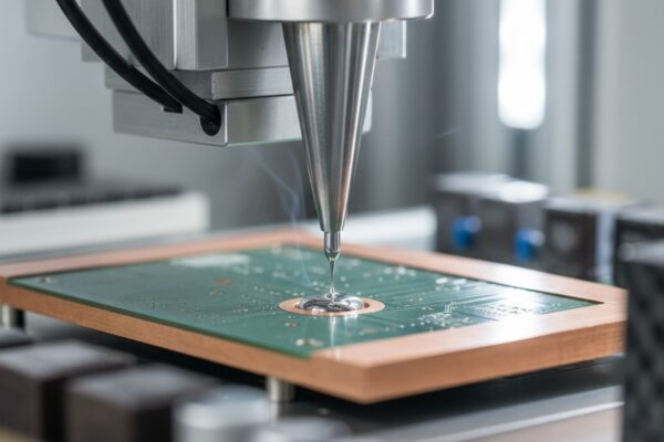
Physics is indifferent to your project deadlines. It doesn’t care about your Bill of Materials target, and it certainly doesn’t care that you saved twenty cents per board by skipping the secondary plating cycle. When you place a via inside a component pad—which modern density often demands—you create a pressure vessel. Treat that vessel casually, like a standard through-hole, and you’re building a microscopic bomb directly underneath your most expensive silicon.
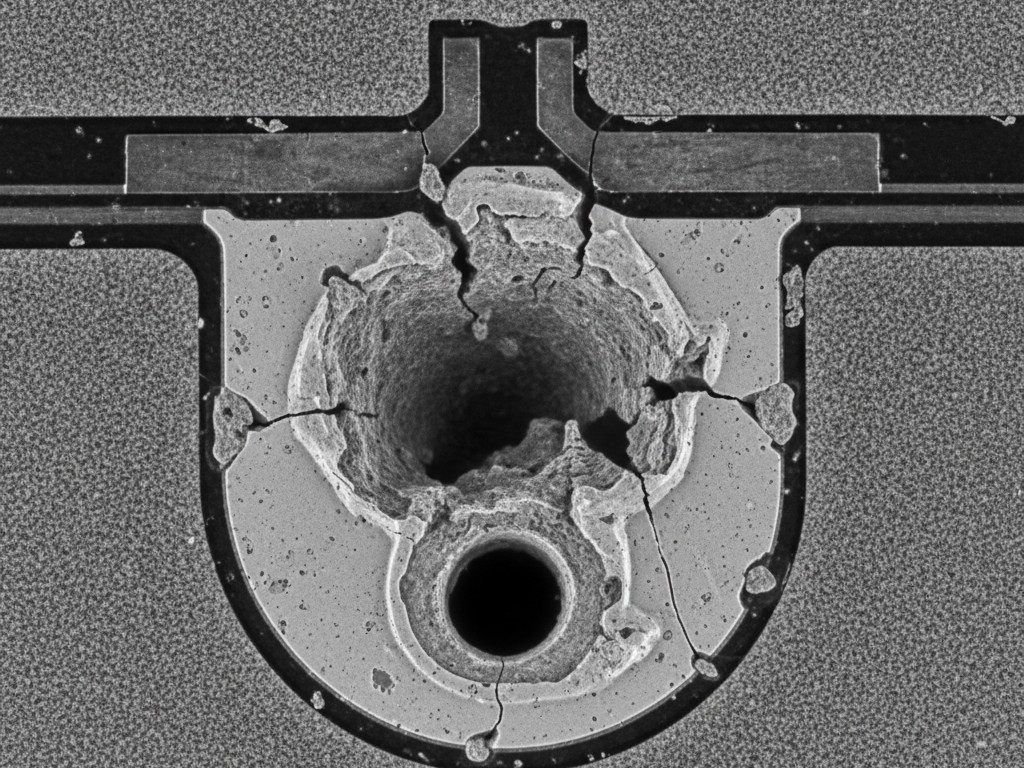
During the reflow process, the temperature ramps past the liquidus point of SAC305 solder (around 217°C) and peaks near 245°C. In that sixty-second window, any moisture, flux vehicle, or air trapped inside that via will expand. Gases expand aggressively. If the via is merely “tented” with solder mask, that thin polymer film stretches like a balloon until it fails. When it bursts, it ejects the molten solder sitting on top of it. The result is a crater in the joint, a lifted component, or a “void” large enough to fail IPC Class 3 inspection. This is the volcano effect. The gas has nowhere to go but up, and it takes your reliability with it.
The Death of the Dog-Bone
There was a time when you could avoid this problem entirely by using “dog-bone” fanouts. You would route a short trace from the BGA pad to a via sitting in open space, keeping the pad solid and the hole separate. That era is effectively over for high-performance digital design.
When you are staring at a Xilinx UltraScale+ or a high-density sensor with a 0.4mm pitch, the geometry to route a trace between pads simply doesn’t exist. A standard 3-mil trace with 3-mil spacing requires more room than the silicon manufacturers have given you. You are forced to drill directly into the pad. Some engineers, perhaps holding onto habits from the 1.27mm pitch era, try shrinking the annular rings to dangerous levels to keep the dog-bone alive, but they’re fighting a losing battle against yield. The drill wander tolerance of a standard mid-tier fab house will eventually bite you. Physics and geometry dictate that the via must go in the pad. The question is no longer “if,” but “how” you fill that hole.
The Illusion of Tenting and Plugging
The most common mistake—and the one causing the most catastrophic field failures—is assuming that standard solder mask can seal a via-in-pad. This is often specified as IPC-4761 Type VI, or “tented and covered.” It’s a seductive option because it costs nothing extra; the CAM engineer simply leaves the mask opening over the via closed.
But Liquid Photoimageable (LPI) solder mask isn’t a structural material. It’s a thin coat of paint. When you tent a via in a pad, you trap air inside the barrel. During that ramp to 245°C, the air expands. The mask softens. The pressure builds until it blows through the molten solder cap, creating the volcano mentioned earlier. Even if it doesn’t explode, the gas bubble can remain trapped in the cooling solder, creating a massive void that acts as a thermal insulator. You have effectively placed your high-power processor on a cushion of air rather than a copper heat path. Tenting is a trap.
Some designers try to get clever by asking for “plugged” vias. They assume “plugged” means the hole is filled solid. In fab-house terminology, however, “plugging” often just means shooting a little extra solder mask into the hole to block the light. It rarely fills the barrel completely. Worse, it creates a non-planar surface. The LPI cures and shrinks, leaving a dimple or depression in the center of the pad.
When the assembly house screens solder paste onto that dimpled pad, the volume calculation is wrong. The paste wicks down into the dimple. The BGA ball, expecting a flat surface, now has to bridge a gap. This leads to “head-in-pillow” defects, where the ball rests on the pad but never actually wets to it, creating an intermittent connection that will pass the factory test but fail the first time the customer drops the device. A plug is not a cap, and a dimple is a defect waiting to happen.
The Only Way Out: Type VII (VIPPO)
The only engineering solution that respects the physics of reflow is IPC-4761 Type VII. In the industry, this is colloquially known as VIPPO (Via-in-Pad Plated Over). It isn’t a single step—it’s a sequence of manufacturing operations designed to turn a hole back into a flat, solid copper pad.
The process begins after the initial drilling and plating. The manufacturer forces a specialized epoxy resin into the via barrel. This isn’t solder mask; it is a dedicated hole-filling compound. Once cured, the board goes through a planarization stage—essentially a mechanical sanding that grinds the excess epoxy flush with the copper surface. Finally, the board goes back into the plating tank. A cap of copper is plated over the filled, sanded hole.
The result is a pad that looks and acts like solid copper. There is no hole for gas to escape from. There is no dimple for solder to wick into. The BGA ball sits on a perfectly flat, conductive surface. The heat from the component travels through the copper cap, into the plating walls of the via, and down to the internal planes. This creates a monolithic copper pad immune to outgassing.
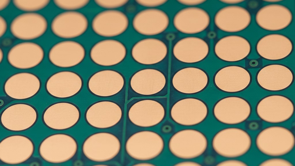
Planarization is the non-negotiable part of this sequence. If you specify “filled via” without specifying “capped and plated over,” you get a barrel full of epoxy with exposed resin on the top. Solder doesn’t stick to epoxy. You end up with a donut of copper with a non-wettable center, which is arguably worse than the dimple. You need the cap.
The Conductivity Myth
When specifying the fill material, you will encounter a persistent debate: Conductive vs. Non-Conductive fill. Many engineers intuitively believe “conductive is better” and specify silver or copper-loaded epoxy, thinking it improves thermal performance. For standard reliability classes, this is almost always a mistake.
Conductive pastes have a Coefficient of Thermal Expansion (CTE) that differs significantly from the surrounding FR4 laminate. As the board heats and cools during operation, the board expands at one rate (Z-axis expansion) and the conductive fill expands at another. This mismatch stresses the copper barrel plating. Over enough thermal cycles, the fill acts like a wedge, cracking the copper knee or separating the plating from the hole wall.
Non-conductive epoxy is formulated specifically to match the CTE of standard Tg170 FR4 laminates. It moves with the board. And regarding the thermal argument: heat transfer in a via happens primarily through the copper plating cylinder, not the core. The difference in thermal resistance between a silver-filled via and a standard epoxy-filled via is negligible for 95% of applications. Unless you are routing 50 amps of DC current where electrical resistance of the barrel is the only metric, the reliability risk of conductive fill outweighs the theoretical gain. Stick to non-conductive fill.
Writing the Fab Note
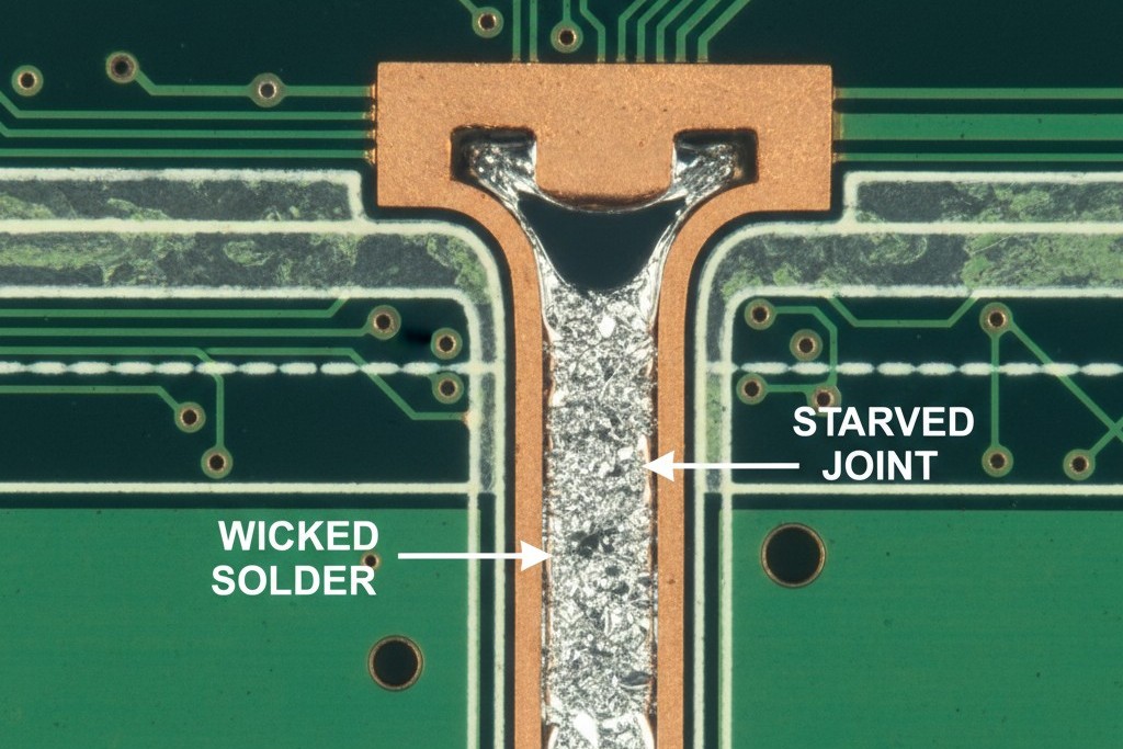
You can’t rely on the CAM engineer to guess your intent. If you simply leave the vias in the pads and send the Gerbers, a conscientious shop will put the job on hold. A budget shop will just process them as open holes, and the solder will wick down the barrel during assembly, leaving the component pin dry—the classic “solder thief.”
You must add a specific layer or a clear text block in your fabrication drawing. It needs to be explicit. Don’t use vague terms like “plugged.” Use the industry standard definition:
“All vias in BGA pads (or specific layers) to be IPC-4761 Type VII. Filled with non-conductive epoxy, planarized, and plated over with min 12μm copper cap. Final surface must be flat and solderable.”
This process adds cost. Depending on the volume and the shop, it can add 15% to 30% to the bare board price because it requires extra plating cycles and manual planarization steps. But you aren’t paying for a hole; you’re paying for the absence of a volcano. Compare that 20% board cost increase against the cost of scrapping a production run of 5,000 units because the QFNs are floating on air bubbles. The math is simple. Physics does not negotiate.

