What is Conductor Side
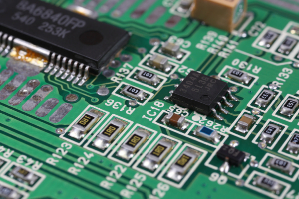
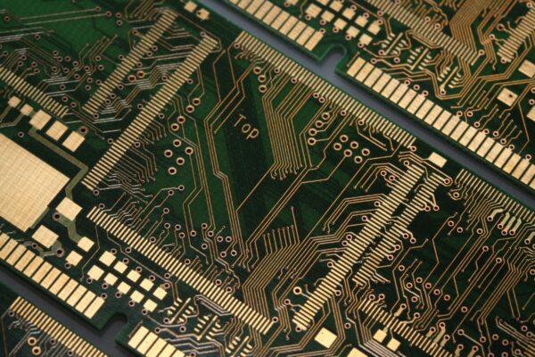
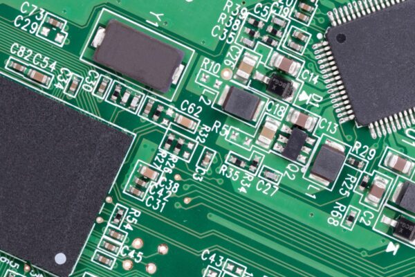
The conductor side is the side of a printed circuit board (PCB) where the conductive copper layer is located. Specifically, in the case of a single-sided PCB, the conductor side is the side of the board where the electrical components are soldered, while the conductive wiring is on the other side.
The conductor side is of utmost importance in the functionality of the PCB as it carries the electrical signals between the components. It is responsible for creating the desired circuit pattern through etching the conductive copper layer, allowing the flow of electricity throughout the PCB.
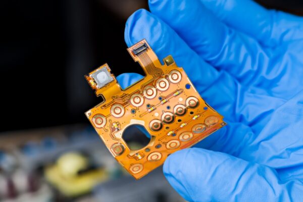
It is worth noting that single-sided PCBs are commonly used in various electronic devices such as calculators, cameras, power supplies, and printers due to their suitability for low-density circuit designs and cost-effectiveness. However, complex circuit designs with space and size constraints may require the use of double-sided PCBs, which have conductive copper layers on both sides of the board.
Frequently Asked Questions
What Are the Components Both Sides of 2 Layer PCB
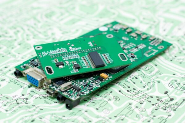
The 2 layer PCB, also known as a double-sided PCB, consists of a printed circuit board with copper coating on both the top and bottom sides. The middle layer is an insulating material commonly used in printed circuit boards. This design allows for layout and soldering on both sides, making it easier to layout and reducing the difficulty of the process. As a result, it is widely used in various applications.
Can You Use Both Sides of PCB
Double sided PCB boards allow for mounting of copper and other components on both sides of the circuit board, which enables the traces to overlap each other. This feature facilitates the creation of more intricate circuits, thereby enhancing the usefulness of the PCB.
