PCB design, an essential part of modern electronics, plays a vital role in shaping our technological landscape. From smartphones to medical devices, printed circuit boards are at the heart of countless electronic products. But what exactly is PCB design?
In this blog, we will delve into the intricacies of PCB design, exploring its fundamental principles, the role of cutting-edge software, the step-by-step design process, and the ever-evolving nature of this critical field. So, whether you’re a tech enthusiast, an aspiring engineer, or simply curious about the inner workings of electronic devices, get ready to unravel the fascinating world of PCB design.
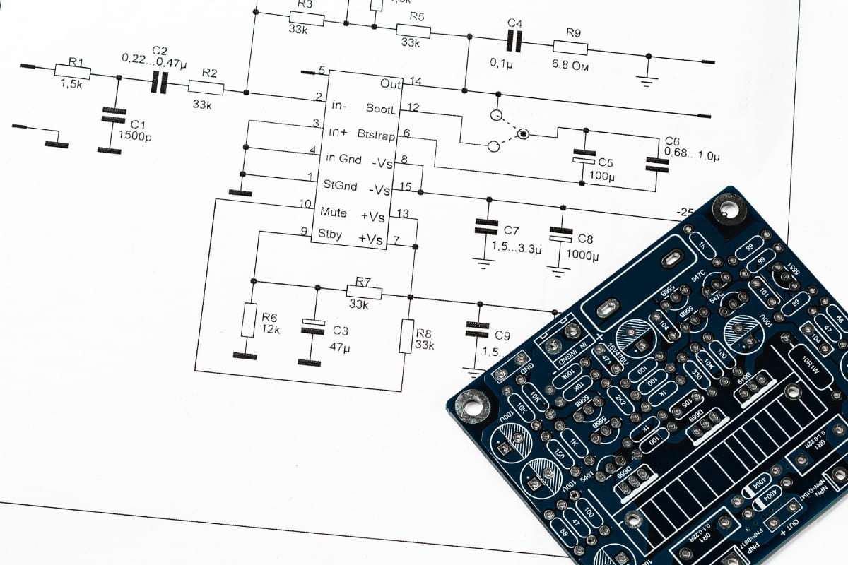
What Is PCB Design
PCB design is the process of creating a layout or schematic for a printed circuit board (PCB). A PCB is a flat board made of non-conductive material, such as fiberglass, with conductive pathways etched or printed onto it. These pathways, also known as traces, are used to provide the electrical connections between various electronic components on the board.
The goal of PCB design is to bring electronic circuit boards to life in their physical form, ensuring that they are functional, reliable, and cost-effective. It is a critical step in the manufacturing of electronic devices, as it determines the functionality, performance, and reliability of the final product.
PCB design is essential to ensure that devices function properly and minimize the risks of electrical shorts, interference, and other problems that can arise with poorly designed circuits.
The Role of PCB Design Software
During the PCB design process, designers utilize PCB design software to create a digital representation of the circuit board to aid in the design process. These software tools provide features for schematic capture, component libraries, and layout design. PCB design software allows designers to place components, such as resistors, capacitors, integrated circuits, and connectors, on the board and define the connections between them.
PCB design software also helps ensure that the layout meets design requirements, such as trace width and clearance between components. They also offer simulation capabilities to verify the design before manufacturing. Utilizing PCB design software streamlines the process and helps ensure accuracy and efficiency.
The advantages of PCB design software include:
Improved Accuracy
Increase the precision of circuit board designs by utilizing PCB design software. This software allows for electronics simulation, reducing the risk of errors and enhancing the reliability of the final product.
Enhanced Flexibility
Say goodbye to the need for physical prototypes and the associated costs. With PCB design software, you can easily modify your designs directly within the software, saving time and money on design iterations.
Streamlined Collaboration
Facilitate collaboration among multiple designers and cross-functional teams with PCB design software. By enabling concurrent work on a design, this software reduces design time and improves the overall quality of the product.
Time and Cost Savings
Take advantage of features like interactive routing, schematic capture, and component libraries to significantly reduce design time. Additionally, PCB design software optimizes component placement and minimizes circuit board size, leading to cost savings during production.
Step-by-Step Guide to Designing a PCB
Designing a printed circuit board (PCB) can seem like a daunting task, but by following these 9 steps, you’ll be well on your way to creating a successful design:
Understand the Electrical Parameters
Before diving into the design process, it’s essential to have a solid understanding of the electrical parameters of the system. This includes factors such as current maximums, voltages, signal types, capacitance limitations, impedance characteristics, shielding considerations, and the type and location of circuit components and connectors. Additionally, having a detailed net wire listing and schematic will provide a clear roadmap for your design.
Create the Schematic
The first step in the PCB design process is creating a schematic. This schematic represents the electrical level of the board’s purpose and function. It serves as a blueprint for the design, outlining the connections between components and their relationships.
Use a Schematic Capture Tool for PCB Layout
To bring your schematic to life, you’ll need to use a schematic capture tool to create the PCB layout. Software platforms like Mentor PADS®, Allegro, or Altium can help you visualize how your board will operate and where the components will be placed. Collaborating with a mechanical engineer at this stage is crucial to ensure the design fits seamlessly into the intended device.
Design the PCB Stackup
Consider the PCB stackup early in the design process. The stackup determines the arrangement of the layers in your PCB and plays a significant role in impedance control. By carefully designing the stackup, you can optimize signal integrity and ensure efficient electrical performance.
Define Design Rules and Requirements
Adhering to industry standards and acceptability criteria is essential in PCB design. Organizations like the IPC provide guidelines that cover various aspects of PCB manufacturing. Familiarize yourself with these standards to ensure your design meets the necessary requirements. Working with a PCB layout provider experienced in IPC standards can help you avoid costly revisions and project delays.
Place Components
Collaborate with your PCB provider to determine the optimal placement of components. Consider design and layout guidelines, as well as any specific requirements for component placement. For example, certain components may need to be isolated from others to minimize electrical noise. The PCB provider will provide data sheets for each component, which will be incorporated into the mechanical layout for your approval.
Insert Drill Holes
Drill holes are necessary for creating connections between layers in your PCB. Ensure that the placement of drill holes aligns with the components and their connections. Double-sided flex circuits, in particular, require careful consideration of drill hole placement.
Route Traces
Once components and drill holes are in place, it’s time to route the traces. Routing involves connecting the various segments of the electrical path on the PCB. Pay attention to signal integrity, impedance control, and minimizing crosstalk during this process.
Add Labels and Identifiers
To enhance clarity and ease of assembly, add labels, identifiers, markings, and reference designators to your PCB layout. These elements help identify specific components and their placement on the board, making it easier for assembly technicians to follow.
Generate Design/Layout Files
The final step in the layout process is generating the design/layout files. These files contain all the necessary information for fabricating and manufacturing your PCB. Once generated, your design is ready to move forward with fabrication, assembly, and testing.
By following these step-by-step guidelines, you can create a well-designed PCB that meets your electrical requirements and manufacturing standards.
PCB Design Best Practices
To ensure a successful PCB design project, it is crucial to establish open and constant communication with the PCB or flex application engineer right from the beginning. This allows you to discuss your project requirements and ensure that both parties are on the same page. Effective communication can greatly minimize the need for extensive revisions later on.
While it is rare for a printed circuit board to be perfectly designed on the first try, maintaining good communication with your PCB provider can help ensure that your design is well-executed from the start. This reduces the likelihood of major revisions that could potentially disrupt your project timeline.
When submitting your design, it is essential to provide accurate information regarding the board size, trace width, materials, component placement, and tolerances. In the case of flex circuits, you also need to determine whether the design is static, partly flexible, or dynamic.
Additionally, it is vital to consider the environmental conditions in which the product will be used. Will the printed circuit board or flex circuit be exposed to non-extreme conditions, such as those found in a cell phone, or will it need to withstand extreme conditions, such as an explosion?
Throughout the PCB design and layout process, you are likely to have questions. Therefore, it is advisable to choose a reputable PCB provider with extensive engineering experience. This ensures that you can rely on their expertise to answer your queries and guide you through a smooth project execution.
By following these best practices and maintaining effective communication with your PCB provider, you can enhance the overall quality of your PCB design and achieve successful project outcomes.
The Evolving Nature of PCB Design
The PCB design process has evolved into a multi-discipline, multi-domain process that requires collaboration, integration, and digital transformation. It involves considering various factors, such as signal integrity, power distribution, thermal management, and electromagnetic compatibility, to ensure the optimal performance of the circuit board.
It is no longer limited to a simple definition but encompasses various aspects of engineering and manufacturing. Working with engineering experts from the beginning is essential to design for manufacturability and ensure a cost-effective and efficient final product. Designers also need to adhere to industry standards and design guidelines to ensure the manufacturability and reliability of the PCB.

 Circuit Board Assembly")


