On the spreadsheet, the Bill of Materials (BOM) always looks perfect. Every row is green, lead times are manageable, and the total cost sits right under budget. But a spreadsheet doesn’t have to survive inside an injection-molded enclosure in Arizona heat, nor does it have to fit onto a physical printed circuit board (PCB) traveling through a reflow oven.
The disconnect between a “parametric match” on a distributor website and the gritty reality of manufacturing is where projects go to die.
Finding an alternate part isn’t as simple as checking a box for “Voltage” and “Resistance.” Algorithms on major distributor sites—whether it’s DigiKey, Mouser, or an automated procurement tool—are designed to sell parts, not to engineer systems. They will happily suggest a “Direct Substitute” for a Texas Instruments voltage regulator based on electrical specs, completely ignoring that the thermal pad on the bottom is a different shape.
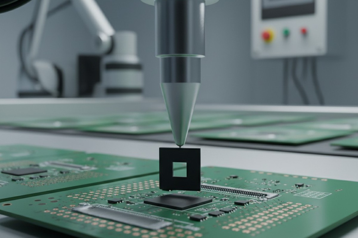
When that board hits the line, the pick-and-place machine doesn’t care about electrical equivalence. It only cares that the part doesn’t fit the landing pattern. You don’t get a warning popup. You get a line-down situation, a pile of scrap, and a very uncomfortable conversation with the VP of Operations.
The datasheet is a legal contract; the web listing is a rumor. Relying on the latter to validate the former is the most common, expensive mistake in the transition from prototype to production.
Geometry is Destiny
The most dangerous assumption in BOM scrubbing is that standard package names imply standard dimensions. In mechanical engineering, a bolt thread is standardized. In electronics, a “QFN-28” (Quad Flat No-leads) package is a suggestion, not a rule.
Say a startup specs a Microchip MCU that suddenly goes out of stock. The procurement team finds an alternate with the same pin count, same voltage, and same “QFN-28” package type. It looks like a drop-in replacement. But if you overlay the mechanical drawings, the reality shifts. The alternate chip might have a thermal pad that is 1.2mm smaller than the original, or a pin pitch tighter by a fraction of a millimeter.
If the PCB footprint was designed for the original, the alternate might technically sit on the pads, but the solder paste stencil will deposit too much solder for the smaller thermal pad. The component floats or tilts during reflow. Worse, the tighter pitch causes microscopic solder bridges that pass visual inspection but short out the moment the device powers up.
This issue extends vertically, too. Engineers often obsess over the X and Y dimensions of a PCB but forget the Z-axis until the board tries to fit into its housing. A shielded power inductor from TDK might be electrically identical to one from Würth Elektronik. But if the TDK part is 1.2mm tall and the Würth part is 2.0mm, that difference is catastrophic if the enclosure has tight clearance. We have seen thousands of units built that simply could not be screwed shut because an alternate inductor collided with the plastic ribs of the case.

Designers often ask if they can rely on the “Drop-in Replacement” tag or “Pin Compatible” flag in search engines. The answer is a qualified “no.” “Pin compatible” usually means the signals are on the same pins. It rarely guarantees the physical body tolerances are identical. A part can be pin-compatible and still be 0.5mm wider—enough to foul against a neighboring capacitor on a dense board. Unless you have physically checked the “Package Outline” section of the datasheet against your Gerber files, you are guessing.
The Invisible Electricals
Once the mechanical fit is verified, the trap moves to the invisible electrical characteristics—data that never makes it into the main filter columns of a search engine.
The classic disaster involves Multi-Layer Ceramic Capacitors (MLCCs). During the great shortages of 2018, panic-buying was rampant. If a Murata 10uF 0805 capacitor was out of stock, buyers grabbed the cheapest available alternate with the same capacitance and voltage rating. The problem is the dielectric.
A capacitor with an X7R dielectric is stable across a wide temperature range. A cheaper alternative often uses Y5V dielectric, which is terribly unstable. At room temperature on a test bench, they behave identically. But put that Y5V capacitor in an outdoor IoT enclosure in the sun, and as the temperature rises, its effective capacitance can drop by 80%. The power rail becomes unstable, the processor resets, and the client wonders why their device fails every afternoon at 2 PM.
For those trying to cut costs, the pressure to switch to “generic” brands is immense. There is a valid time and place for this—a 10k pull-up resistor is largely a commodity, and switching to a generic brand like Yageo or a reputable Asian alternate is usually low risk. But doing this for power components is dangerous.
A generic MOSFET might list the same 30V breakdown voltage, but if you don’t check the “Test Conditions” for the Rds(on) (on-resistance), you might miss that the generic part requires 10V to fully switch on, whereas your board only supplies 3.3V. You end up with a transistor running in the linear region, overheating, and burning a hole through the FR4 material.
Connectors: The Wild West
If integrated circuits are tricky, connectors are the Wild West. There are effectively no standards here. A “JST-style” connector from a third-party vendor isn’t a JST connector. It is a copy, and often an imperfect one.

We encountered a situation with a medical device client who approved a “compatible” header to save lead time. The datasheet looked fine. But the plastic housing on the alternate was 0.1mm thicker than the genuine JST part. When the assembly team tried to plug in the mating harness from the battery, it wouldn’t click. The friction was too high. It required so much force to mate that it risked cracking the solder joints on the PCB. To ship the product, the team had to manually shave plastic off hundreds of headers with X-Acto knives.
This is why connectors are guilty until proven innocent. Unlike a resistor, which can be validated by reading a number, a connector involves haptics, retention force, and plating quality (gold vs. tin). A “compatible” connector might fit physically but use lower-grade plastic that melts during reflow temperatures, or use tin plating that frets and corrodes in high-vibration environments where gold is required. Never approve a connector alternate without holding a sample in your hand and physically mating it with the intended harness.
The Manual Overlay Method
Software can’t save you here. The only reliable validation method is the “PDF Overlay.”
When considering an alternate, open the datasheet of the original part (Part A) and the proposed alternate (Part B) on two separate screens. Scroll immediately to the “Mechanical Data” or “Package Outline” section—usually near the end of the document. Do not look at the marketing summary on page 1. Look at the tolerances.
Check the body width (min/max). Check the pitch. Crucially, check the thermal pad dimensions if it’s a power part. If Part A has a thermal pad that is 4.0mm +/- 0.1, and Part B is 3.5mm +/- 0.1, you have a problem. The solder paste aperture designed for Part A will put down too much paste for Part B, leading to balling or bridging. You also need to check Pin 1 orientation; some manufacturers rotate the die inside the package, meaning Pin 1 is in a different corner relative to the text on the chip.

This process is slow and tedious. It cannot be automated by a script because datasheet formatting is inconsistent. But spending 15 minutes doing a PDF overlay saves weeks of board rework.
Lifecycle and Logic
A part that fits and works is useless if you can’t buy it again. The “Green” in-stock indicator on a distributor site is a snapshot of the present, not a promise of the future.
Before finalizing a BOM, run a lifecycle check. Is the part marked NRND (Not Recommended for New Designs)? If so, the manufacturer is signaling that the end is near. Is the factory lead time 52 weeks? That means the stock you see today is likely the last stock you will see for a year. This is where the panic sets in—the “Stock 0” crisis where buyers are tempted to go to the gray market or unauthorized brokers. While sometimes necessary, this introduces the risk of counterfeits or reclaimed parts. If you must use a broker, the validation burden triples: you now need X-ray and decapsulation testing to prove the chip inside is actually what the label says it is.
BOM scrubbing isn’t about filling rows in a spreadsheet. It is about predicting future failures on the assembly line and preventing them while the design is still digital. It requires cynicism, mechanical awareness, and a refusal to trust the easy answer.


 Circuit Board Assembly")
