What is Die Bonding
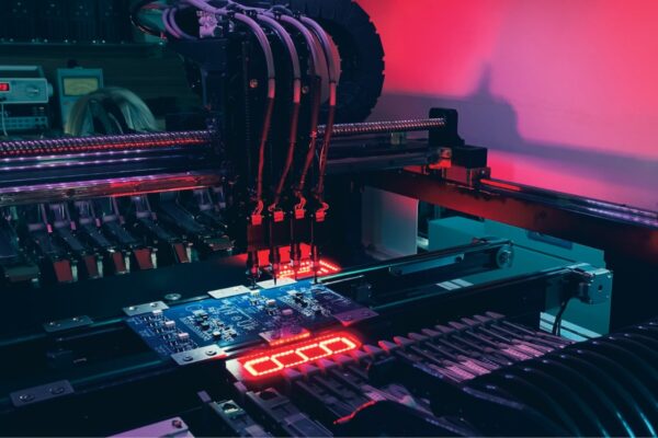
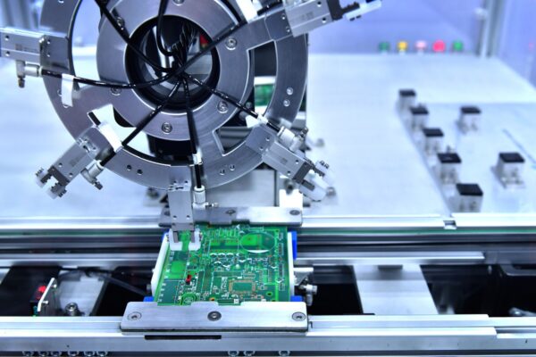
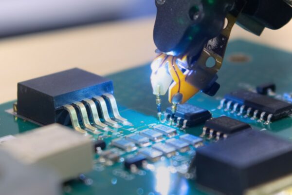
Die bonding, also known as die placement or die attach, is a manufacturing process used in the packaging of semiconductors. It involves securely attaching a die (or chip) to a substrate or package using either epoxy or solder. The die bonding process begins with the selection of a die from a wafer or waffle tray, followed by precise placement onto a specific location on the substrate.
Die bonding is vital in the assembly of electronic components, serving as a bridge between semiconductor manufacturing and semiconductor assembly. It can occur at different levels of electronics assembly, depending on the specific requirements of the product.
At Level 1, die bonding involves interconnecting the bare integrated circuit to its underlying circuitized substrate. The choice of substrate materials, typically ceramic and metal leadframes, is based on thermal (CTE) and reliability considerations. The die is typically bonded on the top side, with interconnection points to the next level on the bottom side, often through pins in through holes. The die bonding material acts as the interconnect layer. Over time, advancements have introduced cavity and bottom side bonding, along with the incorporation of non-active components, passives, and discretes. The end result of this assembly step is the IC package.
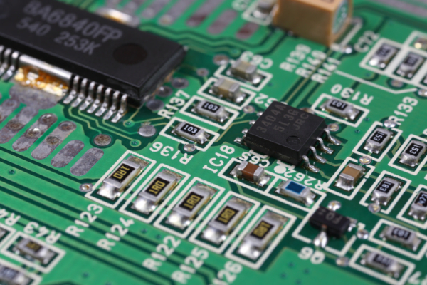
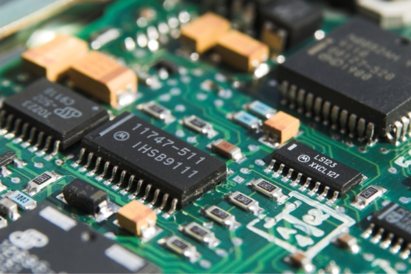
At Level 2, die bonding takes place during the assembly of PCBs. Multiple IC packages, along with capacitors, resistors, and discrete components, are bonded or inserted into the PCB. PCBs typically consist of power and signal layers of etched copper in a fiberglass reinforced matrix, such as FR4. Connection to the next level is established through end-connectors. In certain advanced assembly processes, direct die-to-board bonding is performed, blurring the distinction between Level 1 and Level 2. In fact, in some cases, die are mounted in inner layers of the board as embedded components.
Various die bonding approaches have been developed to meet evolving product requirements. These approaches include epoxy die bonding, eutectic die bonding, and flip chip attachment. Epoxy die bonding involves using epoxy as the bonding material and can be combined with batch, continuous, or in-situ curing methods. Eutectic die bonding entails placing the die into solder (eutectic) for bonding, followed by in-situ reflow. Flip chip attachment involves attaching the die to the substrate or board using flip chip technology and can be combined with standalone or in-situ curing methods.
