The move to 800 V architectures in electric vehicles, energy storage, and industrial power electronics brings clear advantages in efficiency and reduced current. But these benefits collide with a hard constraint: electrical isolation. The separation distances required at 800 V can easily double or triple the footprint of a power board compared to lower-voltage designs. For products where size dictates cost, thermal performance, and market viability, this isn’t a minor inconvenience. It’s a design crisis.
Creepage and clearance are the non-negotiable spacing rules governing high-voltage PCB layout. Mandated by safety standards, both distances grow with voltage and must be satisfied simultaneously. The challenge is not theoretical. An 800 V board can demand clearances over 4 mm and creepage paths beyond 6 mm, consuming area so aggressively that compact form factors become nearly impossible with naive layout practices.
The solution isn’t a single trick. It’s a combination of mechanical intervention through slotting, material science in substrate and mask selection, chemical reinforcement with conformal coatings, and rigorous layout discipline. Each method attacks a different dimension of the spacing problem. Together, they allow 800 V designs to meet safety standards without becoming commercially unviable.
Creepage vs. Clearance: Two Failures, Two Defenses
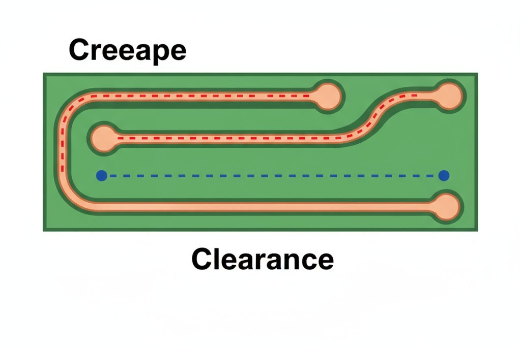
Creepage is the shortest path between two conductors measured along the surface of an insulating material—a purely surface phenomenon. Voltage applied across two points on a PCB will try to form a conductive path along the insulator, typically solder mask or bare substrate. If contamination, moisture, or degradation creates a film on that surface, current can begin to flow in a process called tracking. This current carbonizes the material, creating an increasingly conductive path until a full breakdown occurs. Creepage distance is the defense against tracking.
Clearance, by contrast, is the shortest path between two conductors measured through the air—a volumetric one. Air is an excellent insulator, but only up to a point. When the voltage exceeds the air gap’s dielectric strength, the air ionizes into a conductive plasma and an arc forms. This failure is immediate and catastrophic. Clearance distance is the defense against arcing.
A design can satisfy one and fail the other. A board might have sufficient clearance through the air, yet fail on creepage because a contaminated solder mask provides an easier path for current. Conversely, a clean board might have ample creepage distance but fail on clearance because a tall component obstructs the direct air path, forcing an arc through a shorter gap. Both must be engineered for independently. This dual requirement is the root of the size problem at 800 V, where both distances are large and the larger of the two must be met in every dimension.
How Voltage and Environment Dictate Spacing
Voltage determines the required separation, but the relationship is neither linear nor simple. It is codified in safety standards like IEC 60950-1 and IEC 61010-1, which provide tables mapping working voltage to minimum clearance and creepage. These tables are the result of decades of failure analysis and are legally binding for certified products.
Clearance is governed by Paschen’s Law, which describes the breakdown voltage of a gas based on pressure and distance. For air at standard pressure, the breakdown field is roughly 3 kV per millimeter, but this is only a guide. Standards add safety factors and account for transient voltage spikes that can be several times the nominal working voltage. For an 800 V DC system under Overvoltage Category II, the required basic clearance might be 4 mm or more. This requirement increases at higher altitudes, where lower air pressure reduces air’s dielectric strength.
Creepage is a battle against material degradation. Unlike air, solid insulation breaks down over time when exposed to electric fields, moisture, and contamination. The key metric is the Comparative Tracking Index (CTI), a material property measured in volts that represents its ability to resist tracking. Materials are grouped by their CTI value (I, II, IIIa, IIIb), and standards demand longer creepage distances for materials with a lower CTI.
Decoding the Standards: CTI, Pollution, and Overvoltage
The standards require designers to classify their system based on several factors. The required creepage and clearance distances emerge from the intersection of working voltage, overvoltage category, pollution degree, and material group.
Pollution Degree classifies the operating environment. Degree 1 is a sealed, clean environment. Degree 2, the most common, assumes normal indoor conditions with occasional non-conductive dust or condensation. Degree 3 applies to industrial environments with conductive contamination or persistent moisture. Higher pollution degrees demand greater creepage.
Material Group classifies the CTI of the insulating surface. Group I (CTI ≥ 600 V) offers the best tracking resistance, while Group IIIb (CTI 100-174 V) offers the worst. Standard FR-4 solder mask typically falls into Group IIIa (175-250 V), requiring significant creepage distances. When a conductive contaminant lands on a low-CTI surface, leakage current flows and heats the material, causing carbonization. This carbonized path is more conductive, which allows more current, accelerating the degradation in a self-reinforcing cycle until a permanent track forms. High-CTI materials resist this initial breakdown.
For an 800 V DC design in a typical indoor environment (Overvoltage Category II, Pollution Degree 2) using standard solder mask (Material Group IIIa), the standards might specify a creepage of 6.4 mm or more. These are minimums, not targets. Conservative designs add 20-30% margin, further inflating the required spacing.
The Form Factor Crisis at 800 V
An 800 V system is not a forgiving environment. Under typical conditions, an engineer faces minimums of roughly 4 mm for clearance and 6.4 mm for creepage. These are enormous distances in the world of compact power electronics. A board with just ten high-voltage traces routed in parallel, each requiring 6.4 mm of creepage, consumes 64 mm of width for spacing alone—before accounting for trace widths or component placement.
For a power module meant to fit in a 100×100 mm envelope, allocating over half the area to empty space is untenable. The problem compounds with complexity. A three-phase inverter has at least six distinct high-voltage nets, and the combinatorial spacing requirements can force board dimensions that exceed mechanical or thermal limits.
Products compete on power density, which is limited by volume. A board that is twice the size of a competitor’s requires a larger enclosure, more cooling, and higher material costs. The challenge, then, is to compress the design into the smallest possible area while maintaining full compliance. This requires extending effective distances without extending physical dimensions.
Extending Creepage with Slots and V-Grooves
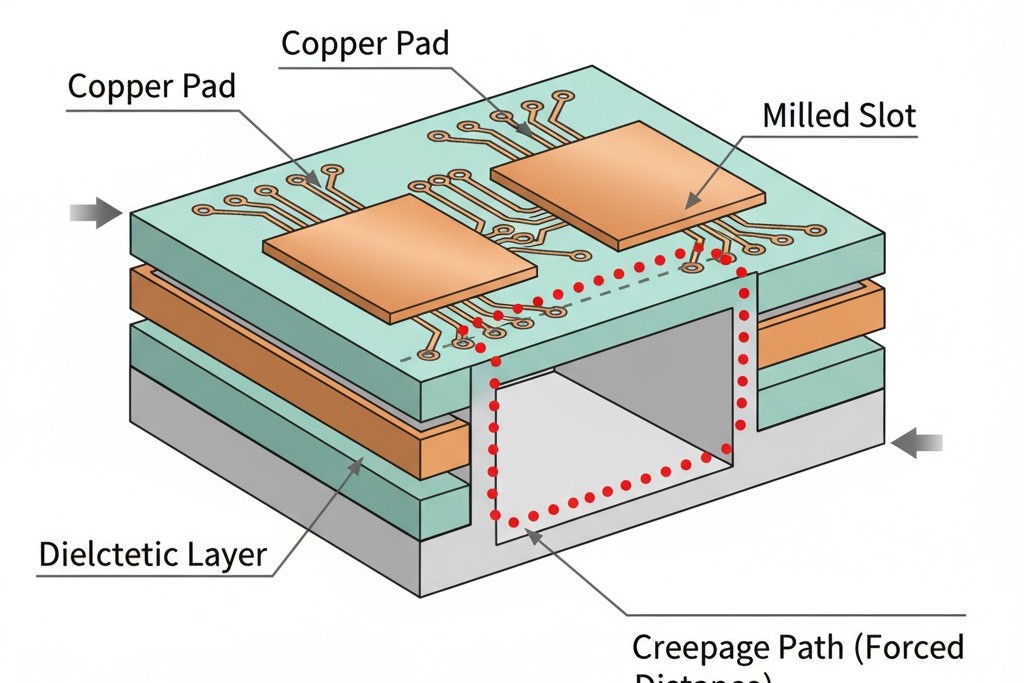
By milling a slot through the PCB, an engineer can force a surface current to travel a longer path around the obstacle. A slot doesn’t change the straight-line distance between two conductors, but it dramatically increases the surface distance a current must travel. Since creepage is defined as the shortest surface path, a well-placed slot eliminates the direct route.
Consider two pads separated by 3 mm. Without a slot, the creepage is 3 mm. By routing a 1 mm wide slot between them that is 3 mm deep, the creepage path is now forced down one wall of the slot, across the bottom, and up the other side. The new path length is roughly 7 mm. The physical separation is unchanged, but the effective creepage has more than doubled.
For this to work, the slot must be deep enough to fully interrupt the surface path, cutting through solder mask and any surface copper. A slot width of 0.5 mm is a practical minimum for most fabricators. However, slots are a creepage-only solution. They do not increase clearance and can, in some cases, reduce it if a tall component body creates a new, shorter path through the air by way of the slot. A design limited by clearance will see no benefit.
The Material Foundation: Choosing High-CTI Substrates
The choice of insulating material is the foundation of a compact high-voltage design. Standard FR-4 laminate has a CTI that places it in Material Group IIIb (100-175 V), the worst category. Standard solder mask is typically only slightly better, falling into Group IIIa (175-250 V). These are the default materials for most fabricators, and they demand the longest creepage distances.
Switching to a higher-CTI material can slash the required creepage. A conductor pair needing 8 mm of creepage on a Group IIIb surface might only require 4 mm on a Group I surface (CTI ≥ 600 V). This is because air itself is effectively a Group I insulator. This creates an opportunity: by using slots or routing traces to the board edge, a designer can replace a low-CTI surface path with a high-CTI air path, often reducing the required distance.
High-CTI solder masks (400-600 V) and laminates exist, but they are premium materials. The designer must weigh the board size reduction against the increased fabrication cost. The conservative approach is to design for standard Group IIIa materials first. If the layout is impossible, upgrading to a high-CTI mask becomes a necessity, not just an optimization.
Conformal Coating: The Chemical Solution
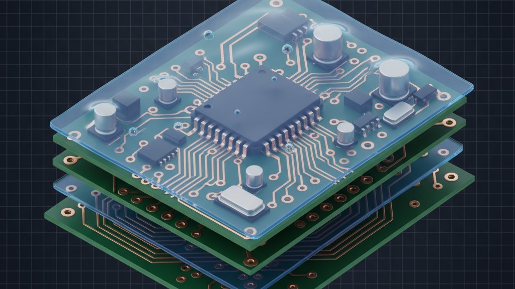
When physical distance is exhausted, a chemical solution remains: conformal coating. This thin, insulating polymer layer is applied over the assembled PCB, conforming to its topography. A properly applied coating acts as a robust insulating barrier, allowing standards-compliant reductions in both creepage and clearance. A coating with high dielectric strength can cut required creepage by 50% or more.
However, standards impose strict requirements. The coating must be rated for the voltage and environment, applied uniformly without voids or pinholes, and remain stable over the product’s lifetime. Common materials include acrylic, urethane, and silicone, while vapor-deposited parylene offers the best but most expensive coverage.
The risk is inconsistent application. Voids, pinholes, or thin spots create weak points where tracking can begin. For this reason, designs relying on conformal coating must be backed by rigorous process controls and inspection. Coating is not a substitute for good layout; it is an augmentation that enables optimization.
Layout and Validation: The Final Discipline
These techniques are useless without rigorous layout discipline. High-voltage design demands that spacing rules are treated as fundamental constraints from the very beginning.
This discipline extends to thermal management. An 800 V board can carry tens of amperes, and the resulting resistive heating requires wide traces, often using heavy copper (2-4 oz). A trace carrying 20 A might need to be 5-8 mm wide to keep temperature rise in check. This width consumes real estate and directly competes with the need for clearance. Spacing between high-current traces serves a dual purpose: it provides electrical isolation and thermal separation.
Design rule checks (DRCs) in EDA software are essential for enforcing keepout zones around high-voltage nets. These rules must be configured manually based on the specific standards, voltages, pollution degrees, and material groups for the project. Crucially, while most tools measure line-of-sight clearance accurately, they often cannot calculate the true surface path of creepage around slots. These critical paths must be verified manually.
Finally, validation closes the loop. It begins with physical inspection of the manufactured boards to ensure slots are clean and coatings are uniform. For the most critical applications, partial discharge (PD) testing provides a higher level of assurance. PD testing applies elevated voltages and uses sensitive detectors to find localized electrical discharges—the precursors to insulation failure. A design that passes PD testing has demonstrated a robust margin of safety, transforming a design crisis into a validated, reliable product.

