In high-mix manufacturing, odd-form components are the enemy of speed. These are the connectors, headers, and heavy transformers that refuse to be surface-mounted, demanding a through-hole process long after the rest of the board has been reflowed.
When faced with a board that is 90% SMT and 10% odd-form through-hole, the instinct is often to route it to a selective soldering machine. It feels precise. It feels modern. It requires zero tooling cost.
It is also, frequently, a trap.
While selective soldering offers programmable precision, it introduces a brutal penalty on throughput. Watching a selective nozzle traverse a board to hit 400 individual points is an exercise in patience that high-volume production lines cannot afford. If a line is running at a 45-second beat rate, a 12-minute selective solder cycle is not a process step; it is a parking lot. The alternative—hand soldering—is even worse, introducing massive labor costs and the inconsistency of human fatigue.

The engineering solution that bridges this gap is the custom wave solder pallet. By shielding the SMT components and exposing only the through-hole pins to the wave, we convert a serial process back into a parallel one. However, designing a functional pallet isn’t just about cutting holes in a sheet of composite material. It is a problem of fluid dynamics, thermal management, and material science. Treat the solder wave as a simple pool of hot metal, and you will design a fixture that creates more defects than it prevents.
Hydrodynamics in a Box
The fundamental challenge of a wave pallet is that it forces molten solder to behave in unnatural ways. A standard wave machine is designed to wash over a flat, open board. When you introduce a pallet, you are asking the solder to flow up into a deep, narrow pocket, wet the joint, and then retreat without dragging the solder back out or leaving bridges behind.
Then there’s the “Shadow Effect.” If the walls of the pallet aperture are too thick, they act like a breakwater. As the board travels over the wave, the leading edge of the pallet wall pushes the solder flow downward, creating a turbulence shadow behind it. The pin sitting in that shadow never sees the wave, resulting in a “skip”—an open joint that requires manual rework. To counteract this, the aperture walls must be chamfered on the solder side to guide the flow up to the pin. Clearing the component isn’t enough. You have to channel the fluid.
There is also the invisible enemy: gas entrapment. Flux generates gas when it hits the preheaters and the wave. On an open board, this gas dissipates upwards. Inside a pallet aperture, specifically one sealing tight against the PCB to protect nearby 0402 resistors, that gas has nowhere to go. It forms a bubble around the joint, preventing the solder from wetting the pad. A properly engineered pallet includes routed gas relief channels—micro-vents that allow the flux fumes to escape without letting the solder in. Without these, you will see perfect-looking joints that are electrically open because they are encased in a microscopic void of rosin vapor.
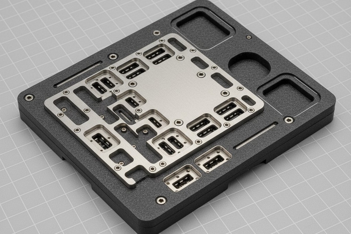
The Material War: Titanium vs. Composite
The primary constraint in pallet design is the “Keep-Out Zone”—the distance between the through-hole pin you need to solder and the nearest SMT component you need to protect. This distance dictates your wall thickness, and your wall thickness dictates your material choice.
If you have 3mm or more of clearance, the choice is simple. Standard composite materials like Durostone or Ricocel work fine. They are cost-effective, easy to machine, and hold up well to the thermal shock of a 260°C solder wave. You can machine a 3mm wall that will survive thousands of cycles without degrading.
That math falls apart when clearance drops below 1mm.
We often see designers place a USB-C connector or a snap-fit clip mere millimeters from a sensitive plastic component. In these scenarios, a composite wall would need to be machined down to 0.5mm or less. At that thickness, composite materials lose their structural integrity. They become brittle, prone to cracking under thermal stress, or worse, they absorb flux and begin to delaminate, turning into a spongy mess after a few production runs.
Enter Titanium Grade 5.
When the clearance is tight, we machine a custom titanium insert and screw it into the composite carrier. Titanium allows for walls as thin as 0.4mm that remain rigid and impermeable to flux. It is an expensive upgrade, often adding $400-$600 to the cost of the fixture, but it is the only way to solder high-density boards without bridging.

There is a valid counter-argument regarding thermodynamics: Titanium is a metal, and metals conduct heat. A large titanium insert can act as a heat sink, stealing thermal energy from the solder joint and causing a “cold solder” defect. This is a real risk. However, it is mitigated by aggressive pre-heating profiles and, counter-intuitively, the thinness of the wall itself. A 0.5mm titanium wall holds very little thermal mass compared to the massive reservoir of the solder wave. The trade-off is almost always in favor of the metal insert when space is at a premium.
Holding Down the Float
Gravity is usually our friend in soldering, but not with odd-form components. Many through-hole connectors, particularly those with plastic bodies, are surprisingly buoyant. When they hit the chaotic turbulence of the wave, they tend to float up. A header that sits flush during assembly might come out of the wave crooked, or “skating” 1mm off the board surface.

A pallet offers a mechanical advantage here that selective soldering cannot: the ability to use “top-hats” or hold-down clips. These are integrated into the top half of the fixture (or a separate lid) to physically lock the component body against the PCB during the soldering process.
If you are dealing with right-angle connectors or heavy transformers, a simple friction fit in the plated through-hole is rarely enough to keep the part true. We have seen entire batches of boards fail quality control because a connector floated 2 degrees off-axis, making it impossible to fit into the final enclosure. A custom pallet with titanium spring-loaded hold-downs solves this mechanically, ensuring that every part sits flush, every time.
The ROI of NRE
The sticking point for most projects is the Non-Recurring Engineering (NRE) cost. A complex wave pallet with titanium inserts and hold-downs can cost between $1,200 and $2,000. For a procurement officer looking at a spreadsheet, that looks like a lot of money compared to the “free” tooling of a selective soldering machine or a roll of Kapton tape.
This is a failure to calculate the Total Cost of Ownership.
Take the “Kapton Tape” trap. It is common to ask if we can simply mask the SMT parts with high-temperature tape and run the board through the wave. The tape is cheap. The labor is not. Applying tape to 500 boards, and then peeling that tape off 500 boards after the wave, is a massive labor sink. It also leaves adhesive residue that requires chemical cleaning. If you are running more than 200 boards, the labor cost of taping will exceed the cost of the pallet.
Similarly, look at the cycle time. If a pallet allows you to solder a board in 45 seconds versus 8 minutes on a selective machine, the fixture pays for itself in machine time alone within the first 1,000 units. The pallet isn’t an accessory. It’s a capital investment in throughput.
When evaluating a new layout, look at the clearances first. If you have the space, standard materials work wonders. If you are tight on space, titanium buys you the margin you need. But do not let the initial tooling cost scare you away from the only process capable of matching the speed of your SMT line.


 Circuit Board Assembly")