What is Tooling Hole
A tooling hole, also known as a fabrication hole, pilot hole, or manufacturing hole, is a strategically placed hole on a printed circuit board (PCB) or a panel of PCBs. These holes serve as reference points for registration and hold-down purposes during the manufacturing process. Tooling holes play a crucial role in ensuring accurate alignment and positioning of the PCBs at various stages of production.
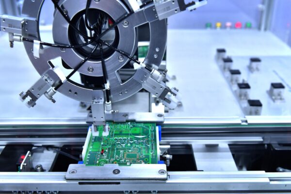
Manufacturers use tooling holes as guides for the placement and alignment of the PCBs on manufacturing equipment such as drilling machines, pick-and-place machines, and assembly fixtures. By utilizing these holes, manufacturers can achieve precise positioning and secure the PCBs during processes like drilling, soldering, and assembly. This helps to maintain the consistency and accuracy of the PCBs throughout the manufacturing process.
Tooling holes are typically small in size and strategically located on the PCB or panel to provide maximum support and stability. They are often placed at the corners or edges of the PCB, allowing for easy and precise alignment. These holes can be designated as plated or non-plated, depending on the specific requirements of the manufacturing process.
The presence of tooling holes enables manufacturers to automate the production process, as machines can utilize these holes as reference points for positioning and alignment. This automation improves efficiency, reduces errors, and ensures consistent quality in the production of PCBs.
Frequently Asked Questions
What Is the Difference Between Supported and Unsupported Holes in PCB
There are two types of mounting holes in PCBs: supported and unsupported. Supported holes are plated and usually connected to the ground plane, while unsupported holes are non-plated and require an outer keep-out zone to prevent interference with other components and traces as they are not connected to a ground plane layer.
What Is the Distance Between Two Holes in a PCB
The distance between two holes in a PCB depends on the type of hole. For PTH, the minimum distance from the bonding pad to the hole to outline should be at least 20mil (D≥20mil). As for NPTH, it is recommended to have a minimum distance of 40mil from the hole to outline (E≥40mil).
What Is the Maximum Hole Size for PCB
The selection of hole size for PCB is not restricted to a specific range, however, there are standard drill hole sizes available to assist in your decision-making process. Opting for a hole size within the range of 5 mil (0.13 mm) to 20 mil (0.51 mm) should be suitable for your design and can be accommodated by your CM. It is important to note that smaller sizes may incur additional costs.
What Is the Smallest Hole in a PCB
The smallest hole size in a PCB is typically 0.0135″. If the drill size is smaller than this, it will be increased to this size. For Prototype PCBs, hole sizes larger than 0.250″ will be finished as non-plated. Holes larger than 0.250″ are considered cut-outs and require different processing.
Are All Holes in PCB Called Vias
There are various types of holes that are drilled into PCBs, including through holes, blind vias, buried vias, and microvias. Through holes are drilled holes that go through all the layers of the PCB, including the conductive and dielectric layers, from one side to the other.
