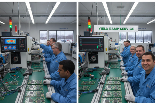
The pressure to shrink product development timelines is relentless, but the consequences of delay have never been higher. Funding milestones slip, market windows close, and competitors ship first. For hardware teams, the gauntlet between a working prototype and a pilot production run—a maze of dependencies, approvals, and fabrication realities—typically spans sixty to ninety days. Speed has always mattered, but is thirty days a realistic target for a complex Printed Circuit Board Assembly (PCBA), or an aspirational fiction that sets teams up for failure?
At Bester PCBA, we know the thirty-day ramp is achievable, but only when three specific systems are optimized in parallel and executed with precision. This isn’t about working faster or cutting corners. It’s about dismantling the structural delays endemic to traditional workflows. The difference between a thirty-day cycle and a ninety-day cycle isn’t effort; it’s the design of the process itself. When a design handoff is clean on the first pass, when fixtureless testing removes the bottleneck of custom tooling, and when Design for Manufacturability (DFM) feedback closes in hours instead of days, the entire critical path compresses. Falter on any one of these, and the timeline cascades into the industry-standard slog.
This is the operational blueprint for that thirty-day execution, a framework built on mechanical realities, not marketing promises. We’ll examine the design handoff that prevents ambiguity, the fixtureless test strategy that eliminates a multi-week delay, and the DFM protocol that keeps engineering feedback from becoming a chokepoint. For teams building complex, multi-layer boards, this is the playbook for de-risking an aggressive timeline while maintaining pilot-grade quality.
Why Thirty Days Is the Exception, Not the Rule
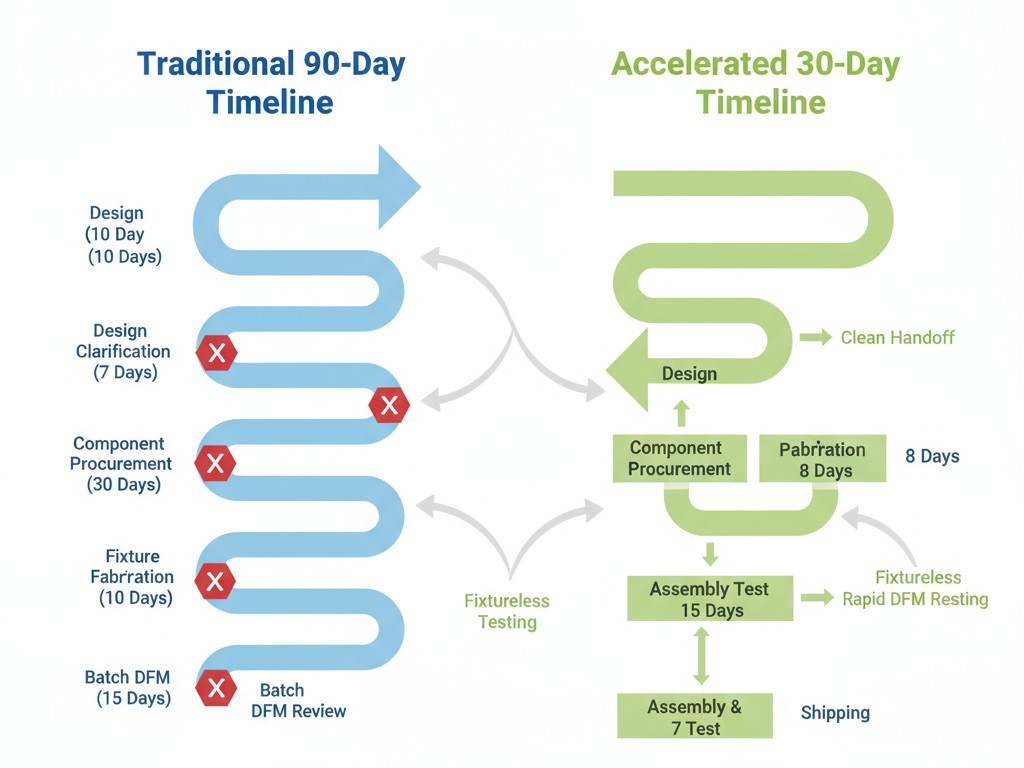
The electronics manufacturing industry’s median time from prototype approval to pilot-ready PCBA hovers between sixty and ninety days. This isn’t because manufacturers are slow; it’s because the process is built as a series of sequential gates, each introducing latency. Incomplete design data triggers clarification loops that add five days before fabrication can even start. Custom test fixtures, essential for traditional validation, carry two- to three-week lead times. DFM feedback, treated as a batch process rather than a continuous dialogue, can burn a week or more.
These delays compound. A two-day slip in DFM feedback pushes the fabrication start date, which delays board delivery, which delays assembly, which delays testing. By the time the pilot build is ready, the thirty-day target has stretched to seventy. The problem isn’t a single vendor or process step. It’s the accumulation of small inefficiencies in a workflow where every stage depends on the last. On the critical path, there is no such thing as a minor delay.
A thirty-day cycle, by contrast, is engineered for zero slack. It demands that every handoff is clean, every process is parallelized, and every decision is pre-resolved. This is why it remains the exception. Most organizations lack the discipline to deliver complete design data on the first pass. Most manufacturers lack the engineering capacity for same-day DFM feedback. Most test workflows are still built around fixtures that require weeks of lead time. The thirty-day ramp isn’t impossible; it is simply unforgiving of the standard inefficiencies that longer timelines are built to absorb.
The Critical Path: Three Gates That Define Your Timeline
Any manufacturing process is governed by its critical path—the sequence of dependent tasks that determines the minimum possible completion time. A delay in any task on this path extends the entire project by the same duration.
For a PCBA pilot ramp, the critical path is controlled by three gates: Design Handoff Precision, Fixtureless Testing Architecture, and DFM Feedback Velocity. These are not independent variables but interconnected systems. Optimizing all three is what makes a compressed timeline feasible. A precise handoff determines when fabrication can start. Fixtureless testing determines when boards can be validated without waiting for tooling. Rapid DFM feedback ensures that design risks are resolved before they cause rework or delays. Together, they form the backbone of the fast-track process.
1. Design Handoff Precision
The first gate is the completeness of the design package. Incomplete data is the single largest source of avoidable delay. When Gerber files are missing layers, a Bill of Materials (BOM) lacks manufacturer part numbers, or assembly drawings are ambiguous, the process grinds to a halt. Engineering teams are forced into a loop of emails and clarification calls, with each cycle consuming at least a day. In a sixty-day timeline, this is an annoyance. In a thirty-day timeline, it’s fatal.
2. Fixtureless Testing Architecture
The second gate is the method for validating assembled boards. Traditional in-circuit test fixtures are custom mechanical assemblies that align spring-loaded probes to test points. They are precise, but they are also slow to produce, requiring up to three weeks for design, fabrication, and debug. This is a three-week serialized process sitting directly on the critical path. Fixtureless methods, like flying probe or boundary scan, eliminate this dependency entirely by using programmable probes or embedded test logic. While throughput may be lower, for pilot volumes of ten to one hundred units, the penalty is negligible compared to the weeks of calendar time saved.
3. DFM Feedback Velocity
The third gate is the speed of Design for Manufacturability analysis. A thorough DFM review catches risks—insufficient clearances, soldermask slivers, poor thermal design—that could cripple yield or reliability. When DFM feedback arrives within hours of design handoff, corrections are made before fabrication begins. When it takes five days, the entire timeline slips by that amount. If the feedback requires design changes, the delay stretches even further.
While component lead times and board complexity also matter, these three gates are the factors most directly controlled by process design. Bester PCBA has optimized them specifically to enable the thirty-day ramp.
The Design Handoff Checklist: Defining “Complete”
“Complete design package” is a common term, but it’s rarely defined with enough precision to prevent ambiguity. A complete package isn’t just a set of files; it’s a guarantee that the manufacturing team can proceed to DFM and fabrication planning immediately, without needing to ask a single question. Incompleteness always manifests in predictable ways: missing drill files, outdated BOMs, mismatched drawings. Each one triggers a query, and each query introduces latency.
Our definition of completeness is a state of zero ambiguity, achieved by adhering to a strict checklist organized around fabrication data, BOM integrity, and assembly documentation.
Gerber Files and Fabrication Data
The Gerber set must include all layers: copper, soldermask, silkscreen, and paste mask, each correctly named. The drill file must specify all hole sizes and plating requirements. The fabrication drawing must lock in board dimensions, layer stackup, material type (e.g., FR-4 or high-frequency laminate), copper weights, and surface finish. For boards with controlled impedance, the stackup must define dielectric thickness, target impedance values, and the specific traces requiring control. Ambiguous fabrication data is the most common cause of delay. When a manufacturer has to guess, the clock is already ticking.
Bill of Materials Integrity
The BOM is the authoritative list of every component to be sourced and assembled. A complete BOM must include reference designators, quantity, manufacturer name, and—most critically—the full manufacturer part number for every line item. A BOM that lists “10k resistor 0402” is not actionable. One that lists “Yageo RC0402FR-0710KL” is, because it specifies an exact, purchasable component.
An incomplete BOM creates two failure modes: procurement delays and assembly errors. Generic part numbers force clarification or risky substitutions. Mismatched reference designators between the BOM and Gerbers lead to misplaced components and rework. Furthermore, integrity extends to availability. A BOM isn’t complete if half the parts have twelve-week lead times. Validating component availability before handoff is non-negotiable.
A thirty-day timeline BOM checklist includes:
- Manufacturer part numbers for all components; no generics.
- Reference designators that exactly match Gerber and assembly files.
- Lead time validation for all components.
- Alternate part numbers for any sole-sourced or high-risk components.
- Clear marking of any customer-supplied components.
Assembly Documentation and Component Placement Files
Assembly documentation includes the assembly drawing, a component placement (or Centroid) file, and any special instructions. The assembly drawing must be a visual reference for the location, orientation, and polarity of every component, generated from the final PCB layout. The placement file provides the X-Y coordinates the pick-and-place machine uses for automation.
Special instructions cover non-standard processes: a connector that must be assembled after conformal coating, a heat-sensitive component requiring a lower reflow profile, or an IC that needs a bake-out due to moisture sensitivity. These details seem obvious to the design team but are invisible to the assembly technician. Complete documentation eliminates interpretation and keeps the line moving.
Fixtureless Test Strategy: Eliminating the Bottleneck
Testing validates that an assembled PCBA works before it moves to the next stage. Traditional manufacturing workflows rely on custom-built test fixtures to provide physical access to test points on the board. For high-volume production, the upfront investment in a custom fixture is justified by its speed and repeatability. For low-volume pilot builds, the fixture is a bottleneck.
Why Traditional Fixtures Break the Thirty-Day Model
A custom test fixture is a mechanical assembly that must be designed, fabricated, and validated before testing can begin. This multi-week process involves analyzing the layout, creating a fixture design, machining the hardware, and debugging the final assembly. For a complex board, this can easily take three weeks.
This is a serialized dependency. Assembly cannot proceed to testing until the fixture is ready. In a sixty-day timeline, a three-week fixture lead time is manageable. In a thirty-day timeline, it consumes half the calendar, leaving no margin for error. The solution is a fixtureless test strategy, which allows testing to begin the moment boards come off the assembly line.
Flying Probe and Boundary Scan as Alternatives

Flying probe test systems use two or more independently controlled probes that move to specific test points to perform electrical measurements. The test sequence is programmed directly from CAD data, so there is no physical fixture to build. Setup time is measured in hours, not weeks. The trade-off is throughput; testing is sequential, so it takes longer per board. For pilot builds of ten to fifty units, this is an overwhelmingly favorable trade-off. A five-minute test that eliminates a three-week wait is an easy decision.
Boundary scan is another fixtureless method that uses embedded test logic within ICs that support the IEEE 1149.1 (JTAG) standard. It allows test equipment to control and observe the state of IC pins without physical contact, which is invaluable for boards with high-density BGAs where test points are inaccessible. Its limitation is that it only works for components with built-in support. For boards with mixed component types, boundary scan is often combined with flying probe to achieve full coverage.
Test Coverage Trade-Offs for Pilot Volumes
Fixtureless testing is not without trade-offs. Test coverage may be lower compared to a full bed-of-nails fixture. For high-volume production, where the cost of a single escaped defect is multiplied by thousands, maximizing coverage is paramount. For pilot volumes, where the primary goal is validating design functionality and catching major assembly defects, the coverage from fixtureless methods is typically sufficient. The key is to choose a test strategy that balances coverage, timeline, and cost for the project’s specific needs, not to default to the traditional approach out of habit.
DFM Response Times: The Feedback Loop That Matters
DFM analysis is how manufacturing engineers find issues that could hurt yield, reliability, or cost. Every board gets a review. The only question is whether it happens proactively, as a structured feedback loop before fabrication, or reactively, as a series of problems discovered on the line that cause delays and scrap. The difference often determines whether a timeline is thirty days or sixty.
What DFM Catches Before Fabrication
A DFM review flags design rules that are technically within spec but leave no margin for process variation, like a trace width that matches the manufacturer’s absolute minimum. The review will recommend a safer dimension that costs nothing but dramatically improves yield. It validates the layer stackup against impedance requirements and checks for component placements that could interfere with tooling or cause reflow defects like tombstoning.
The value of DFM isn’t just identifying problems; it’s identifying them when they are cheap and fast to fix. A trace spacing violation caught in DFM is a one-hour layout change. The same violation caught after fabrication means scrapping the boards and starting over—a two-week delay. This is why DFM response time is on the critical path.
The Engineering Capacity Variable
DFM response time isn’t just a function of design complexity; it’s a function of available engineering capacity. A simple board can be reviewed in hours by an experienced engineer, but it will still take days if that engineer is backlogged.
At Bester PCBA, we structure our engineering capacity to deliver same-day or next-day DFM feedback for fast-track projects. This is a deliberate operational choice, requiring a larger engineering team and disciplined prioritization. It is an investment in speed, and it is a key enabler of the compressed timeline.
How to Act on DFM Feedback Rapidly
The speed at which a design team acts on DFM feedback determines when the board moves to fabrication. The most effective approach is to treat DFM as a synchronous process. When the design is handed off, the team should be ready for rapid iteration. For critical boards, we recommend a live review session where manufacturing and design engineers resolve issues in real time.
Iteration is the enemy of the thirty-day timeline. Each loop adds days. The best way to minimize it is to deliver a clean, manufacturable design from the start, which comes back to the handoff checklist. A clean design leads to minimal DFM feedback, and the loop closes quickly.
Board Complexity and the Feasibility Boundary
The thirty-day timeline is achievable for a wide range of boards, but not all of them. Complexity is the primary variable that determines feasibility. A simple two-layer board can be finished in days. A twelve-layer rigid-flex board with blind and buried vias, impedance-controlled pairs, and 0.4mm pitch BGAs requires longer fabrication cycles and more intensive assembly, stretching the timeline.
- Layer count is the most straightforward driver. A four-layer board takes three to five days to fabricate; a twelve-layer board with blind vias can take ten to twelve. For boards with more than eight layers, the thirty-day window tightens considerably.
- Component density and package types also affect feasibility. A board with 01005 passives and 0.4mm pitch BGAs requires tighter process control during reflow and increases the risk of defects that demand rework.
- Impedance control adds fabrication complexity and DFM risk. It requires precise material thickness and validation, and if the impedance is out of spec, the boards must be scrapped and re-fabricated.
The goal isn’t to discourage complex designs, but to set realistic expectations. For a six-layer board with standard components, a thirty-day ramp is conservative. For a ten-layer board with dense BGAs and tight impedance tolerances, it’s achievable but demands flawless execution with zero margin for error.
Executing the Thirty-Day Ramp: An Integrated Framework
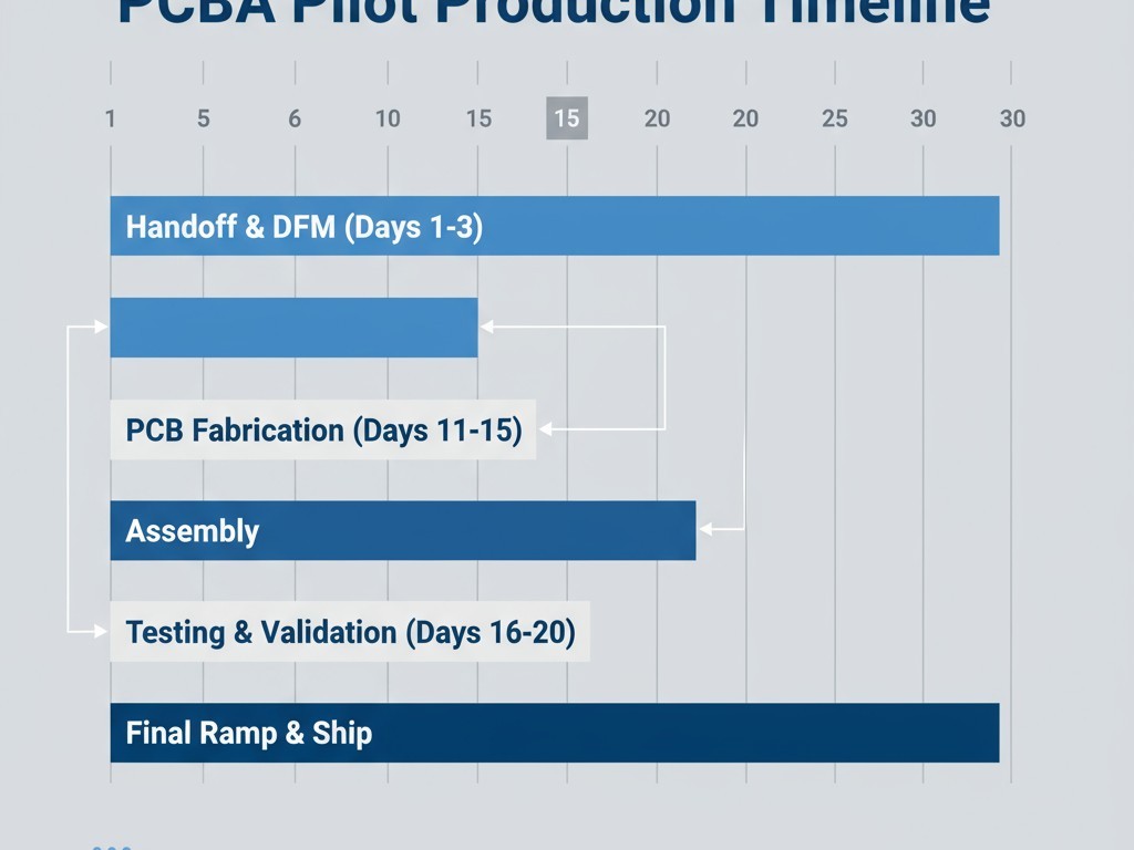
The thirty-day timeline is a tightly choreographed sequence. This framework outlines a realistic day-by-day progression for a complex six- to eight-layer board with a pilot quantity of twenty to fifty units.
Days 1–3: Handoff and DFM On day one, the complete design package arrives. DFM review begins immediately. By end of day two, feedback is delivered. On day three, the design team submits corrected files, and the board is cleared for fabrication. This phase is where the handoff checklist proves its worth; an incomplete package can stretch this phase to a week, immediately killing the timeline.
Days 4–10: PCB Fabrication Fabrication begins on day four. For a six-layer board, this involves imaging, lamination, drilling, plating, and finishing. This part of the timeline is the least compressible, as it is dictated by physical processes. Bare boards ship to the assembly facility on day ten.
Days 11–15: Assembly Component kitting and stencil fabrication happen on day eleven. Solder paste printing, pick-and-place, and reflow occur over the next two days, followed by any manual assembly. Inspection is completed on day fifteen. The biggest risk here is component availability, which is why lead time validation during handoff is non-negotiable.
Days 16–20: Testing and Validation Fixtureless testing begins on day sixteen, as soon as boards are available. Assembly defects are identified and reworked over the next few days. Because no custom fixture is required, this phase starts immediately after assembly. With traditional fixtures, testing wouldn’t begin until day twenty-five or later.
Days 21–30: Pilot Ramp and Final Validation By day twenty-one, initial boards have been tested and the assembly process refined. The remaining pilot units are built, tested, and validated. Final inspection, packaging, and shipment occur by day thirty. The product team now has functional pilot units in hand, having saved three weeks compared to a traditional cycle.
The critical dependencies are clear. DFM must close by day three. Fabrication must finish by day ten. Fixtureless testing must begin by day sixteen. Each gate enables the next. When all three systems are optimized, the thirty-day timeline isn’t a stretch goal. It is the natural outcome of a well-designed process.

