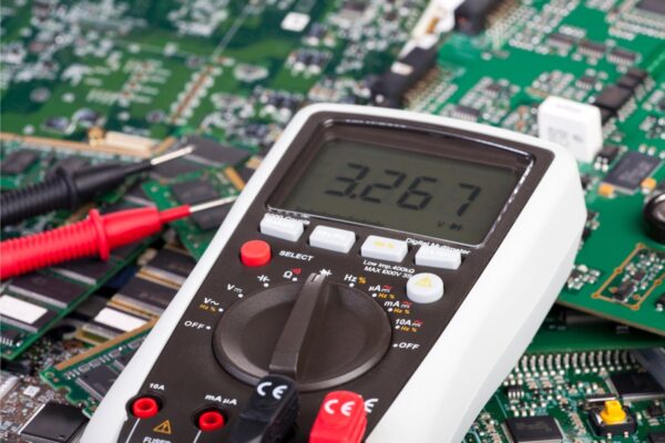
You have likely held that one perfect board in your hands. It arrived via express courier, meticulously packaged in anti-static bubble wrap, smelling faintly of isopropyl alcohol and triumph. It booted up on the first try. The LEDs blinked in the correct sequence. The voltage rails sat rock-steady at 3.3V. You signed the approval form, authorized the production run of 5,000 units, and went to sleep thinking the hard part was over.

Six weeks later, you are standing in a warehouse looking at pallets of dead inventory. The production units are failing at a rate of 15%. The contract manufacturer (CM) points at your signature on the First Article Inspection (FAI) approval, claiming they built exactly what you approved. Technically, they might be right. The disaster didn’t stem from a bad design. It happened because the “Golden Sample” was a lie. It was likely hand-assembled or reworked by a master technician who compensated for a drifting pick-and-place machine or a cooling reflow oven. The sample proved the design could work, but it proved nothing about whether the process was stable.
The Lie of the Checkbox
The standard industry FAI report is a bureaucratic shield, not an engineering tool. It usually arrives as a PDF containing a list of component designators—R1, C4, U2—next to a column of checkmarks labeled “Pass.” This document tells you absolutely nothing. A checkbox won’t reveal that a capacitor is technically within tolerance but skirting the very edge of failure. It won’t tell you that the solder paste printing was insufficient but just “good enough” to survive a single power-on test. It is a binary simplification of an analog reality.
When you rely on a binary “Pass/Fail” report, you accept a black box. You trust that the vendor’s definition of “Pass” aligns with your product’s long-term survival. Often, it does not. In consumer electronics, a “Pass” might mean the component is present and the solder joint is shiny. But if you are building medical IoT devices or automotive sensors, “shiny” is not a metric. You need to know if the 10uF capacitor is actually 10uF, or if it is a cheaper 8.2uF substitute that will derate and fail once the device heats up.
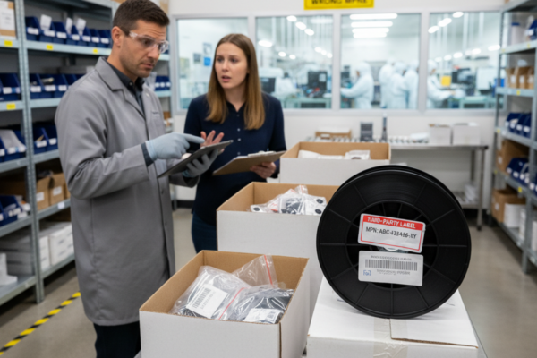
This is where supply chain anxiety should trigger a demand for data, not just assurance. If you are worried about counterfeit parts or silent substitutions—a valid fear in the current shortage climate—a checkmark offers zero protection. Only raw data exposes the swap.
The Truth is in the Drift
Real engineering validation requires measured values. A Bester PCBA FAI report differs from the standard because it provides actual parametric data from the LCR meter for passive components. This distinction sounds subtle, but it separates a prototype that works by luck from a product that works by design.
Consider the “Silent Cap Swap” scenario. You specify a high-grade Murata capacitor with a specific Equivalent Series Resistance (ESR) to handle ripple current in a power supply. The CM, facing a shortage, swaps it for a generic alternative with the same capacitance but double the ESR. A standard continuity check says “Pass.” The device powers on. But the ripple current generates excess heat, cooking the board from the inside out over three months.
If you had the measured values, you would see the fingerprint of the swap immediately. An LCR meter reading doesn’t just confirm capacitance; it reveals the secondary characteristics that define component quality. When you see a row of 10k resistors measuring exactly 9.98k, 9.99k, and 10.01k, you know the process is under control. If you see them measuring 9.5k, 10.5k, and 9.1k, they are technically within a 5% tolerance, but the variance screams that the reel is low-quality or the machine feeder is unstable.
This data allows you to make decisions before the boards even arrive. In high-frequency RF designs, for example, the inductance values in the matching network are critical. If the FAI report shows the inductors are consistently reading on the low side of the tolerance range—say, 1.8nH instead of 2.0nH—you can adjust your firmware trim values to compensate before you even unbox the hardware. You stop reacting to failure and start engineering around a known variable.
The Invisible Solder Joint
Visual inspection is functionally useless for modern electronics. If your board contains a Ball Grid Array (BGA) or a Quad Flat No-Lead (QFN) package, you cannot see the most critical connections. They are hidden beneath the component body. A technician with a microscope can inspect the outer fillet of a QFN, but they cannot see the ground pad underneath, which is responsible for 80% of the thermal dissipation.
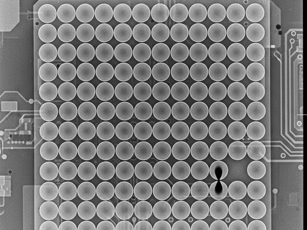
You must demand X-ray transparency. Without it, you are gambling on the reflow profile. A common defect in BGAs is the “head-in-pillow” failure, where the solder ball deforms but doesn’t fully coalesce with the paste. Electrically, it might make contact for the First Article test. But after thermal cycling—turning the device on and off a few dozen times—the joint cracks and the board dies. This is the root cause of those maddening “intermittent failures” that plague field units, where a device works until you tap it or heat it up.
A proper FAI report includes automated X-ray inspection images and, crucially, voiding percentage data. The IPC-A-610 standard allows for some voiding (gas bubbles in the solder)—typically up to 25% depending on the class. You don’t need zero voids; physics rarely allows for perfection. But you need to know if you are at 5% or 24%. If the report shows your main FPGA has 22% voiding on the power balls, that board is a ticking time bomb, even if it passed the functional test. X-ray images turn a “black box” process into a quantifiable risk assessment.
Validating the Machine, Not the Hand
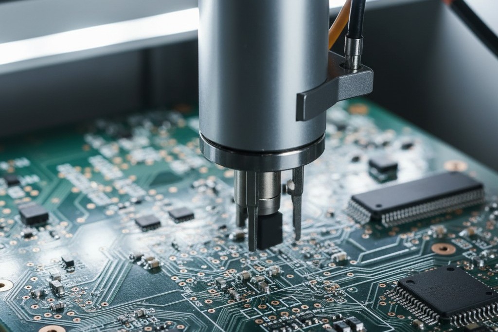
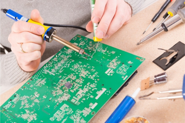
The ultimate goal of the First Article Inspection isn’t to verify that one board works. It is to verify that the machine can build 5,000 of them without human intervention. The “Golden Sample” trap works because a skilled human can fix a machine’s mistakes on a single unit. They can hand-tweak a tombstoned 0402 resistor, reflow a cold joint with a hot air station, and clean the flux residue until it looks perfect.
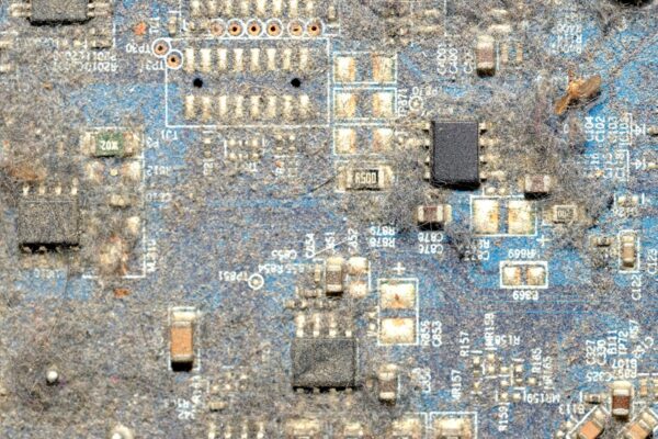
You need to see the raw evidence of machine placement. Look for photos that show the component alignment relative to the pads before reflow, or high-magnification automated optical inspection (AOI) images. If the parts are consistently skewed 10 degrees to the left, the pick-and-place machine is drifting. A human might nudge them back into place for the sample, but the machine will not do that for the production run.
When you review the FAI, you are auditing the process. You are looking for proof that the reel tape was loaded correctly, that the nozzle size was appropriate for the package, and that the reflow oven’s zone temperatures matched the profile. If the vendor cannot provide data proving the machine did the work, assume the sample was hand-built.
Engineering Proactivity
If you are reading this, you already know what the acronym FAI stands for. What matters is shifting the mindset from “receipt of goods” to “receipt of data.”
Treat the FAI report as a debugging tool, not a shipping document. When you receive a Bester PCBA report populated with measured values, X-ray density maps, and high-resolution placement photos, you are holding the health metrics of your entire future production run. Use that data to tighten your tolerances, adjust your thermal management, or disqualify a component vendor who is shipping out-of-spec parts. The cost of analyzing a PDF is minutes; the cost of reworking 5,000 units is a career-ending event.


