Cold joints in heavy copper assemblies are not a soldering skill problem. They are a thermal energy problem. When your PCB design pushes copper weights to three ounces per square foot or beyond, when power planes sprawl across entire layers, and when busbars integrate directly into the stackup, the physics change. Standard reflow profiles and wave solder processes were designed for boards with modest thermal mass. They assume heat applied to a component lead will propagate quickly, bringing the joint to its liquidus temperature within a predictable window.

Heavy copper shatters that assumption. The copper itself becomes a heat sink so massive it starves the joint of thermal energy. You’re left with dull, grainy surfaces and incomplete intermetallic bonds that fail in the field or trigger expensive rework loops before the board ever ships.
At Bester PCBA, we treat heavy copper and high-current builds as a thermal management challenge first and a soldering process second. The solution isn’t just higher solder pot temperatures or longer dwell times. It’s a system-level strategy: understand the physics of thermal mass, apply aggressive and precisely controlled preheating, and tailor the process profile to the thermal inertia of your assembly. This is how you avoid the defects that plague heavy copper builds and deliver boards that meet Class 2 or Class 3 reliability standards without endless rework.
Why Heavy Copper Defeats Standard Soldering Processes
The problem is thermal inertia. Copper’s high specific heat and thermal conductivity mean that when you move from one-ounce to four- or six-ounce copper, you aren’t just scaling the geometry—you’re multiplying the thermal mass. This mass acts like a sponge for heat, absorbing vast amounts of energy for even a modest temperature rise. When a solder wave or reflow oven applies heat, the massive copper plane conducts it away from the joint faster than the source can replenish it. The joint never reaches the solder’s liquidus temperature, or it gets there so briefly that a reliable metallurgical bond can’t form.
A cold joint is a failure of intermetallic compound formation. When molten solder meets a copper surface at the right temperature, a thin layer of intermetallic compounds—primarily Cu₆Sn₅ and Cu₃Sn—forms at the interface. This layer is the bond. Its formation requires both sufficient temperature and sufficient time. If the copper surface never gets hot enough because its own mass has drained the available energy, the intermetallic layer is incomplete or absent. The result is a joint that looks superficially wetted but lacks structural integrity. Under thermal cycling or mechanical stress, these joints crack. Under electrical load, they exhibit high resistance and generate heat, accelerating failure.
The visual tells of poor thermal transfer are obvious: a grainy or dull solder surface, poor fillet formation, and none of the smooth, concave meniscus of a properly wetted joint. These are the signatures of solder that solidified before it could do its job. While IPC-6012 defines these defects for Class 2 and Class 3 boards, the standard doesn’t tell you how to avoid them. That requires engineering the process to overcome the thermal deficit.
This challenge scales nonlinearly. A two-ounce board might tolerate a standard reflow profile with minor tweaks. A four-ounce board will produce defects unless the process is fundamentally redesigned. A six-ounce board, or one with integrated busbars, can defeat even the most aggressive process changes. The first step is recognizing that thermal mass isn’t a detail. It is the central constraint.
Copper Weight Specifications and Their Thermal Implications
Copper weight is specified in ounces per square foot, a measure of thickness. One ounce of copper is about 1.4 mils (35 microns) thick. Six ounces is 8.4 mils. The difference seems small, but its impact on thermal mass is huge. Because mass scales with volume, a six-ounce copper plane has six times the mass of a one-ounce plane of the same area. It has six times the thermal inertia and requires six times the energy to reach the same temperature.
For assemblies in the one- to two-ounce range, standard reflow or wave soldering processes usually provide enough heat. The thermal mass is manageable, and the board reaches equilibrium within a typical cycle. Minor adjustments to soak time or peak temperature might be needed, but the process remains conventional.
At three to four ounces, the thermal landscape shifts. The copper begins to dominate the assembly’s thermal budget, and standard convection heating can no longer keep up. Preheat becomes essential. Without it, the board enters the reflow zone with significant thermal gradients; the copper is far cooler than the components. Solder paste melts, but the joint forms incompletely because the underlying copper never reached liquidus temperature. At this weight, process modifications are no longer tweaks—they are requirements.
At six ounces and above, or in assemblies with large busbars, the thermal mass becomes extreme. Conventional reflow and wave processes, even with extended preheat, simply cannot deliver enough energy. The copper acts as an infinite heat sink. These assemblies often demand selective soldering with extended dwell times, hand soldering with high-thermal-capacity irons, or alternative techniques like induction heating. Understanding where your design falls on this spectrum dictates the entire manufacturing strategy, starting with the most critical step: preheating.
Preheat Strategies for High-Mass Joints
Preheating isn’t just about warming the board; it’s the most powerful tool for managing thermal mass. Its purpose is to shrink the thermal gap between the copper and the target reflow temperature, minimizing the energy needed during the final soldering stage. A standard assembly might be preheated to 120–140°C. For heavy copper, the target must be far higher—often 160–180°C or more—to ensure the copper’s inertia doesn’t create a thermal deficit that the reflow zone can’t overcome. This requires both higher temperatures and longer soak times to let the mass equilibrate.
Bottom-side infrared (IR) and forced convection are the most effective methods. Infrared heating delivers radiant energy directly to the copper surfaces, which are highly absorptive. This allows energy to penetrate the board and heat internal layers more effectively than convection alone. Forced convection complements IR by ensuring uniform air temperature, reducing the risk of cold spots. For heavy copper work, wave solder systems need extended preheat zones with multiple IR emitters, and reflow ovens need their preheat zones extended or their IR elements upgraded.
Soak time—the duration the board spends at peak preheat temperature—is not a luxury. It is a necessity. Without an adequate soak, the board’s surface and components might reach the target temperature, but the bulk copper mass will lag behind. A proper soak allows heat to conduct throughout the copper, eliminating these gradients. A four-ounce board might require a 60- to 90-second soak at 160°C. For six-ounce or busbar-laden assemblies, soak times can extend to two minutes or more.
The trade-off of aggressive preheating is the risk to thermally sensitive components like electrolytic capacitors or plastic-housed connectors. Prolonged exposure to 180°C preheat can degrade these parts. The solution is zoned preheating, where heat is focused on the heavy copper areas while shielding sensitive components. This is inherent to selective soldering, but in reflow, it may require custom fixtures or accepting a narrower process window.
Many facilities try to process heavy copper boards in standard reflow ovens. This is possible for moderately heavy copper (around three ounces) but requires meticulous profile development and often results in marginal yields. The primary limitation is preheat power. Standard ovens simply lack the IR density to bring heavy copper to temperature quickly enough. Slowing the conveyor helps but kills throughput. If your oven cannot deliver 160°C or higher to the copper mass with an adequate soak, the process will fail. At that point, selective or hand soldering becomes the only reliable path.
Selective Soldering for Mixed Thermal Mass Assemblies

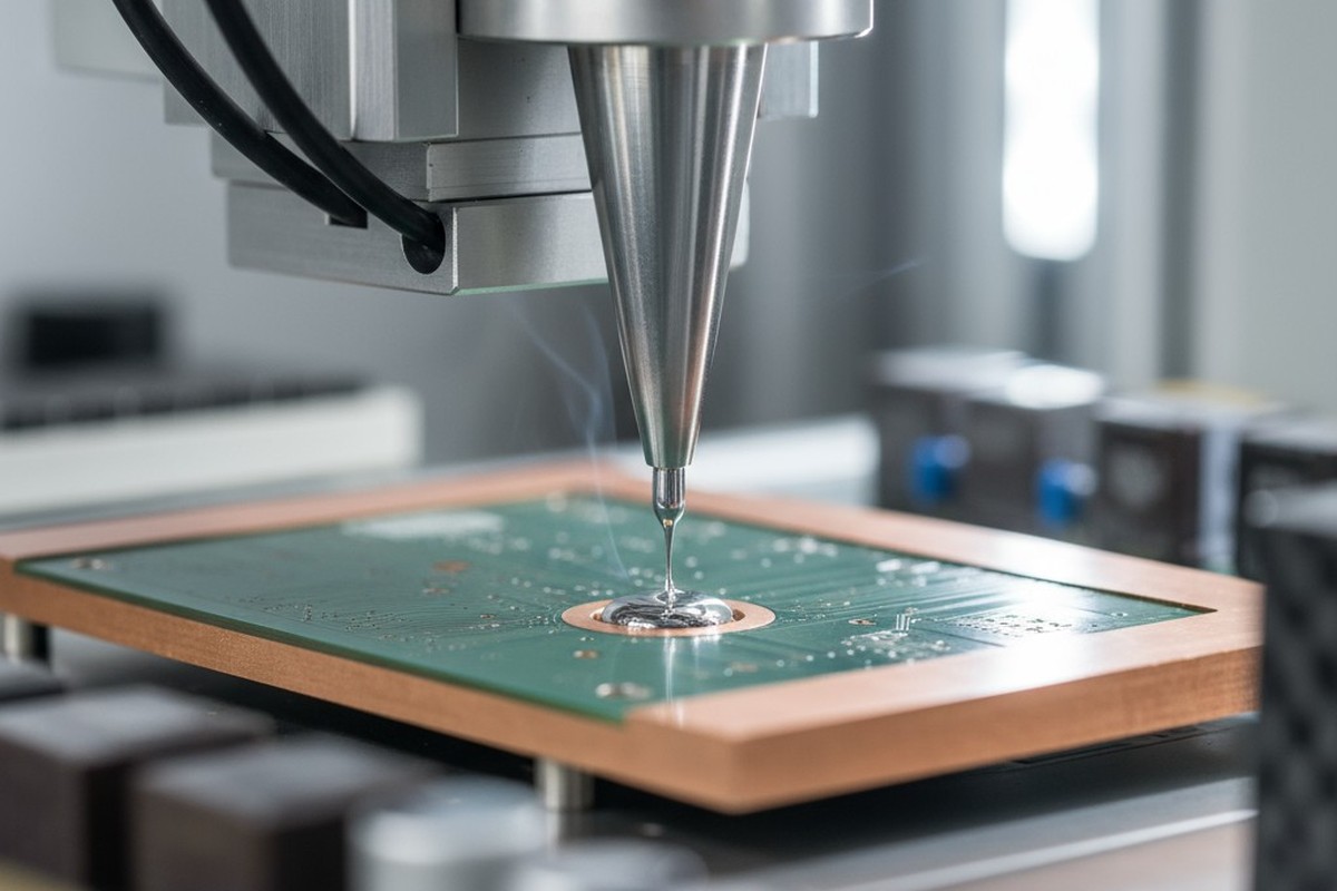
Selective soldering applies molten solder to specific joints using a small nozzle, rather than immersing the entire board in a wave. This precision makes it invaluable for assemblies with mixed copper weights—where heavy power planes coexist with standard signal layers—or when through-hole components in high-mass areas must be soldered without cooking the rest of the board. The advantage is precision; the disadvantage is throughput.
Selective soldering is the right choice when thermal mass varies significantly across the board, when sensitive components can’t tolerate a global preheat, or when board geometry makes wave soldering impractical. A power supply with a six-ounce power section and a two-ounce control section poses a dilemma for wave soldering: a profile aggressive enough for the heavy copper will overheat the light copper, while a conservative profile will create cold joints. Selective soldering solves this by treating each zone independently. The six-ounce area gets localized, extended preheat and a longer solder contact time, while the two-ounce area receives standard treatment.
The key is to achieve thermal equilibrium in the high-mass zone without overheating the low-mass zone. This is done with zone-specific preheat using IR or hot air nozzles positioned over the target area. The preheat can be ramped to 180°C for the heavy copper zone, while the rest of the board stays at a lower temperature. The solder nozzle then applies solder with an extended dwell time to ensure complete wetting despite the copper’s residual heat-sinking.
Nozzle selection and dwell time are critical. The nozzle must match the joint geometry. For heavy copper, a larger nozzle or a mini-wave provides a greater volume of molten solder, which acts as a thermal reservoir to sustain heat input. Dwell time—the duration of contact—must also be extended. Where a standard joint might need one or two seconds, a heavy copper joint may need three to five seconds or more. Flux must also be managed carefully, as localized, extended heating can deplete its activity and lead to poor wetting.
Wave Soldering High-Current Boards
Wave soldering remains a viable process for heavy copper boards, but only if they have uniform thermal mass. Its advantage is throughput, making it economical for volume production. The challenge is that the entire process must be tuned to the worst-case thermal mass on the board. If the copper is uniformly heavy, this works. If it varies, you risk overheating the light areas or underheating the heavy ones.
Extended preheat zones are essential. A standard wave solder machine might have a 1.5-meter preheat section; for heavy copper, 2 meters or more with at least four zones are often required. This provides the time and energy necessary for the copper mass to equilibrate. The target temperature at the exit of the preheat section should be 160–180°C, measured directly on the copper surface with contact thermocouples, not inferred from air temperature.
Conveyor speed determines the contact time with the molten solder wave. Standard speeds of 1 to 1.5 meters per minute are often too fast for heavy copper. The copper’s heat-sinking effect can pull the joint temperature below liquidus almost immediately. Slowing the conveyor to 0.6 to 0.8 meters per minute extends the contact time, allowing the joint to stabilize and complete intermetallic formation. The trade-off is lower throughput. Finding the optimal speed requires iterative testing with thermocouples to confirm the joint reaches and sustains the target temperature.
Thermal Profile Design Principles
A thermal profile is the board’s time-temperature journey. For heavy copper, you can’t just scale a standard profile; you have to architect a new one that accounts for the immense thermal lag of the copper mass.
High-mass profiles require extended soak durations and potentially higher peak temperatures. The soak zone, where the board is held just below the solder’s melting point, allows the copper to equilibrate. For a four-ounce board, a 60-second soak might need to become 90 or 120 seconds. The soak temperature should be as high as components can tolerate—often 160–170°C—to minimize the remaining gap to liquidus. The peak temperature may need to be pushed to the upper limit of the solder alloy’s specification, such as 250°C for lead-free SAC305, just to ensure the heaviest copper areas reach liquidus.
Validating the profile with thermocouples attached directly to the heavy copper areas is non-negotiable. A profile validated by measuring air or component temperature is meaningless. You must measure the copper itself. Run the board through the process and analyze the data. The copper must reach liquidus and stay there for at least 45–60 seconds for leaded solder or 60–90 seconds for lead-free. If it falls short, adjust the profile—increase preheat, extend soak, or raise the peak temperature—and test again.
Insufficient time above liquidus is the most common failure. The copper hits liquidus for a moment, but its own thermal inertia pulls the temperature back down before the metallurgical reactions complete. This creates weak joints with incomplete intermetallic layers. Other profile-related failures include bridging, often caused by flux depletion from excessive preheat, and excessive flux residue from a profile that is too long or too hot for the flux chemistry.
Busbar Integration and Extreme Copper Features
Busbars are solid copper bars used to carry currents of tens or hundreds of amperes. Their thermal mass is orders of magnitude greater than even the heaviest copper planes. Soldering to a busbar is beyond the capability of any conventional reflow or wave process; it requires localized, sustained heat that can overpower the busbar’s ability to conduct it away.

Techniques for busbars include high-thermal-capacity soldering irons, resistance soldering, and mini-wave solder pots. A standard soldering iron will fail because the busbar pulls heat away faster than the iron can supply it. A high-capacity iron, with a massive tip and over 150 watts of power, can sustain the necessary heat input. The technique involves preheating the busbar with the iron for 10–20 seconds before applying solder. Mini-wave or fountain solder pots are also effective, delivering a localized stream of molten solder that acts as both the bonding material and a thermal reservoir.
Fixturing is critical to prevent misalignment from thermal expansion. Custom fixtures that clamp both the busbar and the PCB are a must. Preheating the entire assembly in an oven before localized soldering also helps by reducing the overall thermal gradient.
Joint inspection for these high-reliability applications must be rigorous. Visual inspection must confirm complete fillet formation, a smooth concave meniscus, and a shiny surface. For Class 3 applications, cross-sectional analysis is often required on first articles to provide definitive proof of a robust intermetallic layer.
Avoiding Rework Loops Through Process Validation
The goal of all this work—optimizing preheat, selecting processes, and designing profiles—is to eliminate defects before they happen. Rework is expensive, risky, and a sign of a broken process. The only way to avoid it is through empirical process validation using test boards that replicate the thermal mass of your production design.
Embed thermocouples in the highest-mass areas of these test boards. Run them through the proposed process, capture the data, and analyze the curves. Verify that every critical joint reaches and holds its liquidus temperature for the required duration. If any area falls short, adjust one variable—preheat temperature, soak time, conveyor speed—and retest. This data-driven, iterative approach builds a process that works. The investment in test boards is trivial compared to the cost of scrapping production units.
After soldering, visual inspection should focus on the tell-tale signs of proper thermal transfer. Good joints show complete wetting, with solder flowing smoothly into a concave fillet. The surface will be shiny, not dull, grainy, or fractured. Poor joints, where solder beads up or looks frosted, are the signature of insufficient heat. They are a prediction of field failures. Catching them in validation lets you fix the process at its source.
Validated thermal management is the thread connecting every part of this guide. Whether designing a preheat strategy or soldering a busbar, the challenge is the same: deliver enough thermal energy to the copper mass to form a complete intermetallic bond. The validation step confirms you’ve succeeded. When the data shows the copper gets hot enough and the inspection shows it wetted properly, you have a process that will eliminate cold joints, rework loops, and field failures.


 Circuit Board Assembly")

