You have likely stood in a conference room, staring at a projector screen showing a hazy, low-contrast image from a unit that just came off the line. The electrical tests passed. The functional checks passed. The board powers up, the sensor initializes, and the data flows. Yet the image looks like it was shot through a dirty window.
The immediate reaction from procurement is to blame the glass vendor for a defective coating or the sensor manufacturer for a bad batch. But if you are looking at a sealed optical unit—whether a LIDAR module, automotive camera, or medical endoscope—the culprit is rarely the glass. It is the invisible chemistry happening five millimeters away on the printed circuit board.
The gap between “clean enough for electrons” and “clean enough for photons” is where millions of dollars in inventory go to die. In standard electronics manufacturing, cleanliness is defined by resistance. If the residue left on the board doesn’t conduct electricity across the pads, the board is considered clean. This is the logic of IPC-610 and standard J-STD-001 protocols.
Optics, however, don’t care about resistance; they care about volatility. A residue that is perfectly electrically benign can still be chemically active, waiting for a trigger to lift off the board and redeposit itself on the coolest surface nearby. In a sealed housing, that surface is always the inner side of your lens.

Firmware teams often misdiagnose this as sensor noise. Engineers will spend weeks tweaking ISP algorithms, increasing black levels, or fighting fixed-pattern noise that seems to drift over time. If you see noise that correlates with device temperature or operating time, stop coding. You aren’t fighting gain. You are fighting a physical layer of polymerized smog that has condensed directly onto the microlenses of your CMOS sensor. No amount of code can clean a physical contaminant.
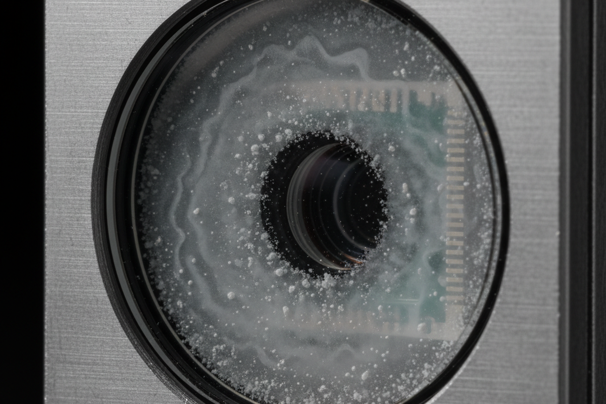
The Chemistry of the Sealed Chamber
The primary offender in this drama is “No-Clean” flux. The name itself is one of the most dangerous misnomers in the optical supply chain. “No-Clean” does not mean “No-Residue”; it means the residue left behind is non-corrosive and electrically safe to leave on the board. In an open-air environment, like a consumer router, this is fine. The volatiles gas off into the room, and the solids stay put.
But an optical module is a closed ecosystem. When you seal a PCB inside an IP67 housing, you create a micro-climate.
Consider the physics when that unit powers up. Processors and power management ICs heat up. The air inside the housing expands, and vapor pressure rises. The “benign” flux residue on the solder joints—specifically the bromide activators and rosin carriers—begins to outgas. It doesn’t need to boil; it just needs to sublimate. These microscopic particulates float through the internal convection currents of the housing.
Eventually, the unit powers down. The housing cools. The glass window, being the thinnest barrier to the outside world, cools first. The vapor condenses on that cold glass, forming a haze that is often invisible to the naked eye but opaque to a laser or sensor.
We have seen this play out in high-stakes environments, such as LIDAR units for autonomous trucking. A unit might pass every test on the factory floor, but after a 200-hour burn-in, the window develops a milky film. Mass spectrometry often reveals this isn’t a defect in the glass coating, but a layer of polymerized flux rosin that migrated from a “clean” solder joint inches away. This isn’t a failure of the flux to do its job. It is a failure of the engineer to understand that a sealed optical unit is effectively a distillation chamber.
Some engineers try to solve this by applying conformal coating, assuming that sealing the board will trap the nastiness. This often backfires. If you coat a board that hasn’t been chemically stripped of residues, you are essentially trapping moisture and solvents against the laminate. When the board heats up, those volatiles expand, creating bubbles or delamination. Worse, the coating itself can outgas if not properly cured. You cannot seal away dirt; you have to remove it.
Heat is the Prosecutor

Residue is patient. It can sit harmlessly on a board for months, only to cause a field failure when the seasons change. This is why thermal cycling is not optional for optical products. If you are only testing image quality at room temperature in a lab, you aren’t validating the product. You are only validating its dormancy.
The failure mode often looks like “ghosting” or soft-focus that appears only in hot environments—say, a security camera mounted in Phoenix in July—and disappears when the unit cools down. This is the signature of mobile residue. At 60°C, the viscosity of certain flux residues drops, allowing them to creep. Alternatively, the heat drives the outgassing rate up exponentially. By the time you get the unit back to the failure analysis lab, the residue may have re-solidified or the volatiles may have dispersed, leaving you with a “Could Not Duplicate” resolution.
You must stress the system to see the dirt. Thermal cycling acts as an accelerated aging process for contamination, forcing migration that would otherwise take six months to happen in six days. If you aren’t running your optical qualification units through a -40°C to +85°C cycle while monitoring image quality, you are flying blind.
The Washing Paradox
The logical reaction to the “No-Clean” problem is to demand that the contract manufacturer (CM) wash the boards. “Just run them through the aqueous cleaner,” you say.
This is where the second trap opens up. Washing a board is high-risk; do it incorrectly, and you are arguably worse off than if you had left it dirty.
Imagine a standard inline wash system. It sprays hot water and a saponifier (chemical soap) onto the board to dissolve the flux, rinses it with deionized water, and dries it with air knives. It sounds perfect. But walk the floor of a contract manufacturer in Suzhou or Guadalajara and look at the wash tank. If the line manager is cutting costs, that tank might be saturated with dissolved flux. It becomes a bath of dirty water, spraying your boards with a concentrated solution of the very contaminants you are trying to remove.
When a board goes through a dirty wash, or if the rinse water isn’t monitored for turbidity, you get residues that are far more insidious than the original flux. Saponifiers have low surface tension; they love to creep under low-standoff components like BGAs or QFNs. Once trapped there, the air knives can’t dry them out. You end up with a pool of conductive sludge hidden under your main processor. Over time, this causes dendritic growth—metal whiskers that grow between pads and short them out.
This leads to the “Defective Lens” blame game. You see a spot on the image and reject the lens vendor’s lot. But if you tear down the unit, you might find that the “fungus” on the lens is actually a dendrite that grew from a trapped pocket of detergent, migrated across the PCB surface, and encroached on the optical path. A saturated wash tank deposits more dirt than it removes, and it deposits it in the places you can’t clean.
Redefining “Clean” for Optics
To solve this, you have to stop relying on standard industry crutches. IPC-610 Class 3 is a workmanship standard, not an optical cleanliness standard. It will tell you if your solder joints are shiny and if your components are straight. It will not tell you if the board will fog your lens.
You need to move from global testing to local testing. The industry standard for cleanliness is the ROSE test (Resistivity of Solvent Extract), which dunks the whole board in a solution and measures how much the resistivity drops. It gives you an average cleanliness score for the entire surface area. This is useless for optics. You can have a perfectly clean board with one heavy smudge of flux right next to the image sensor. The ROSE test averages that smudge out to zero, but the sensor sees it as a catastrophic failure.
The solution is to specify “Optical Cleanliness” in your drawing notes. This means demanding localized Ion Chromatography (IC) testing on the critical areas surrounding the sensor. It means specifying the exact allowable limits of specific ions—chloride, bromide, sulfate—rather than a generic “pass/fail.” It means auditing the wash process to ensure turbidity sensors are active and that the wash chemistry is changed based on board volume, not just calendar days.
You cannot rely on the “standard process” to protect your optical system. The standard process is designed for things that don’t see. If you want a clear image, you have to treat the PCB not just as a circuit, but as an optical component in its own right.


