In high-reliability manufacturing, there is a dangerous comfort in the green checkmark. A batch of heavy-copper boards for an EV traction inverter rolls off the line, passes Automated X-ray Inspection (AXI), and ships to the customer. The paperwork is pristine. The IPC-A-610 Class 3 requirements—often revered as the gold standard—have been met. Yet, three months later, those same boards fail in the field, thermal cycling themselves to death because the power FETs are delaminating. The disconnect here isn’t a failure of the machine to measure. It is a failure of the standard to account for physics. A board that is legally safe can still be physically doomed.
The problem often lies in how we define a “good” solder joint for power components. Standard inspection algorithms focus heavily on total void percentage—calculating the volume of gas trapped in the solder relative to the total pad area. If the spec allows 25% voiding and the machine measures 18%, the board passes. But thermodynamics does not negotiate with percentage points. We have analyzed field returns where that “acceptable” 18% voiding wasn’t scattered randomly; it was pooled directly under the silicon die’s hot spot, acting as a perfect thermal insulator. The heat, unable to move through the void, spiked the junction temperature (Tj) well beyond the safe operating area. The percentage was fine, but the location was fatal.
The Flat Earth Problem: Why 2D X-Ray Misses the Point
These defects slip through largely because of the tools used to grade them. Many contract manufacturers still rely on standard 2D transmission X-ray systems. These machines project X-rays through the entire thickness of the board and capture the resulting shadow on a detector. While adequate for checking shorts on a simple resistor, this approach flattens the world of a complex power assembly into a single plane. On a double-sided board, components on the bottom interfere with the image of the top, creating a noisy, ambiguous picture that algorithms struggle to interpret.
The issue compounds when dealing with BGAs or BTCs (Bottom Termination Components) where the vertical structure of the joint matters. In a 2D image, a void appears as a light spot, but the image cannot tell you where that void sits vertically. Is it a harmless bubble in the bulk of the solder, or is it a “planar void” essentially disconnecting the component interface? We have seen cases misdiagnosed as “insufficient solder” where the voiding was concentrated entirely at the intermetallic interface, creating a weak mechanical bond and a thermal bottleneck. Without 3D capabilities like Laminography or Computed Tomography (CT) to slice the data into layers, an inspector is essentially guessing at the integrity of the thermal path. You cannot grade what you cannot see in three dimensions.
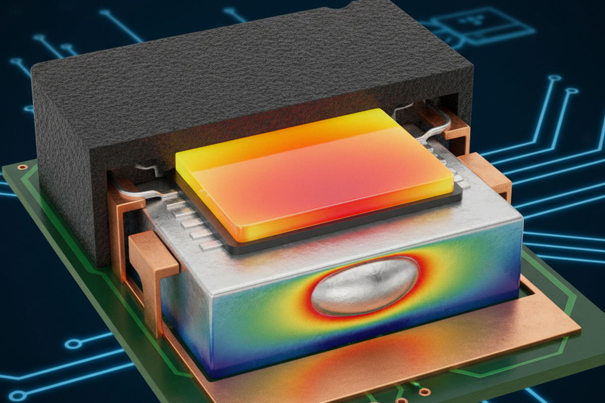
Thermal Topology: Location Trumps Percentage
When the goal is heat dissipation, void topology matters infinitely more than total volume. Think of the thermal path as a highway for heat, traveling from the die, through the die attach, into the leadframe, through the solder joint, and finally into the PCB thermal pad and vias. A void is a roadblock. If you have ten small voids scattered around the periphery of a D2PAK thermal pad, the “highway” is still open in the center, and heat flows efficiently from the source. This scenario might technically register as 15% voiding. Conversely, a single large void centered directly under the die might only register as 8% total voiding, but it blocks the primary arterial route for heat flux.

This distinction is critical for high-power density parts like IGBTs or high-brightness LEDs. In one analysis of streetlights failing prematurely, the driver boards showed voiding levels that were technically passing standard inspection criteria. However, thermal imaging revealed junction temperatures spiking 30°C higher than the design limit. The voids were acting like “Swiss cheese” in the worst possible arrangement, increasing the thermal impedance ($R_{th}$) of the joint. Granted, the solder joint is only one link in the chain; if the external heatsink surface isn’t flat or the Thermal Interface Material (TIM) is poorly applied, a perfect solder joint won’t save the board. But as PCBA process engineers, the solder interface is the variable we control. Ensuring a continuous thermal path is the only metric that counts.
A Better Grading Heuristic
Moving beyond the “checkbox” mentality requires a grading strategy based on thermal continuity rather than simple void limits. Bester PCBA advises dropping the binary “Pass/Fail” based on a single percentage number in favor of zone-based grading criteria for power pads. This involves defining a “critical zone”—typically the center 50% of the thermal pad where the die sits—and applying much stricter voiding limits to that specific area, while allowing looser tolerances on the periphery.
This approach requires more sophisticated programming of AXI equipment, but it aligns inspection criteria with physical reality. We look for “interfacial contact area”—the amount of guaranteed solder connection directly under the heat source. There is no magic number that applies to every design; a low-power logic chip might survive with 40% voiding, while a GaN power transistor might fail with 10% if it’s in the wrong spot. Grading must be context-aware. If the algorithm cannot be tuned to this level of nuance, the “gray area” results—boards that are technically passing but look suspicious—should be flagged for manual review by a technician who understands the thermal path, rather than being auto-passed.
Prevention at the Source
The best way to grade a void is to prevent it from forming in the first place. High void counts on thermal pads are rarely random accidents; they are usually the signature of a process or design violation. The most common culprit is stencil design. A large, open aperture for a QFN thermal pad allows too much paste to be printed, which then outgasses during reflow. If that gas has nowhere to escape, it forms a giant void. The standard fix is “window-paning” the aperture—breaking the large square into smaller squares with gaps in between—to create channels for volatiles to escape.

The design of the bare PCB plays an equally massive role. We frequently see designers placing open, unfilled vias inside the thermal pad. During reflow, gravity and capillary action pull the hot solder down into these holes—a phenomenon known as solder wicking—leaving the component floating on insufficient solder. This leads to massive voiding and poor connection. If thermal vias are required in the pad, they must be tented on the back side or plugged and capped to prevent this theft of solder. No amount of X-ray grading can fix a board where the solder has physically drained away.
The Verdict
Reliability isn’t a certificate you hang on the wall. It is the physical ability of a device to survive its operating environment. Adhering strictly to IPC Class 2 or 3 voiding limits provides a legal shield, but it doesn’t change the laws of thermodynamics. For power electronics, standard grading criteria are often insufficient. By shifting the focus from “total void percentage” to “thermal path integrity,” and by utilizing 3D inspection tools that reveal the true structure of the joint, we can stop shipping boards that are destined to burn. The cost of a more rigorous inspection is always lower than the cost of a recall.


 Circuit Board Assembly")