What is Air Gap
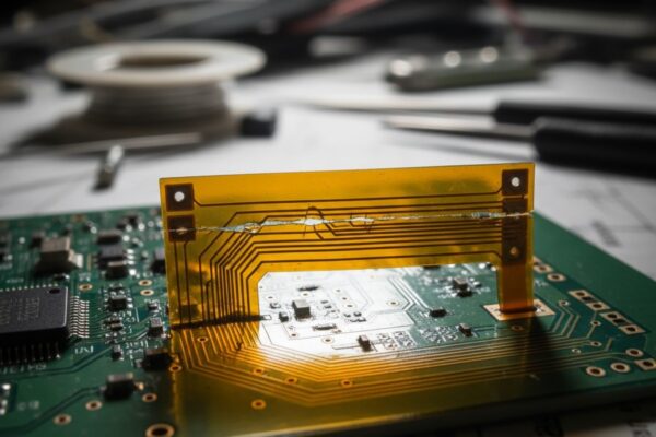
In a PCB, an air gap is a deliberate separation or distance between different layers or components of a printed circuit board. It is a construction technique that involves creating empty spaces or gaps within the PCB structure. The purpose of introducing an air gap in the construction of a PCB is to address via reliability concerns and improve the overall reliability and performance of the board.
By incorporating air gaps, the bending stress on the PCB is distributed more evenly, reducing the strain on vias and improving the overall reliability of the PCB. This construction technique also helps to eliminate concerns related to via plating, as the need for vias can be minimized. Additionally, air gaps provide insulation and prevent potential short circuits or interference between different layers of the PCB.
The specific configuration and placement of air gaps can vary depending on the design requirements of the PCB. They can be strategically placed between ground and power planes to ensure electrical separation and maintain signal integrity. The presence of air gaps in a PCB design indicates a need for isolation and electrical separation between different layers, which is important for reducing noise, preventing voltage conflicts, and ensuring the overall functionality and reliability of the PCB.


