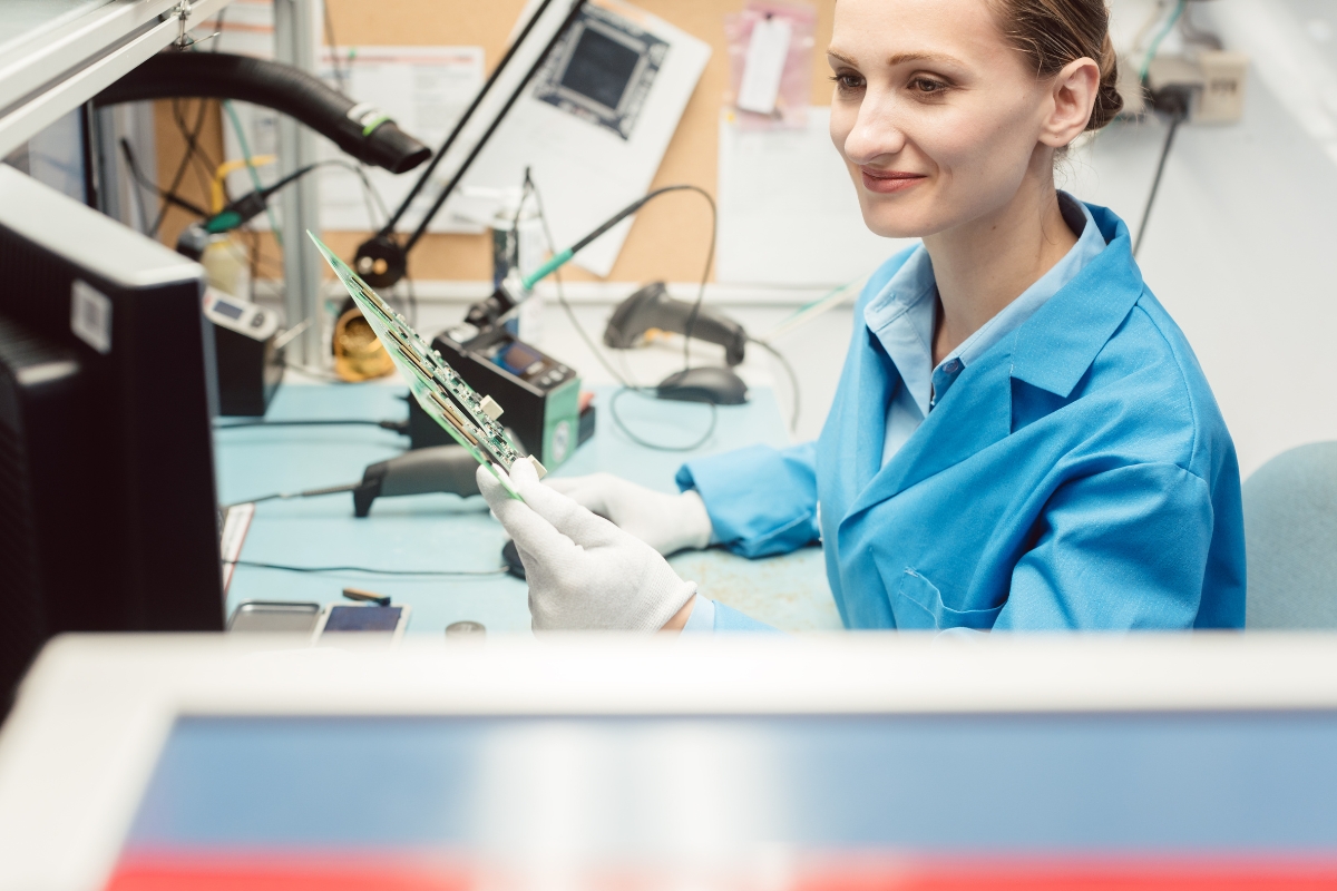
What Is PCBA Testing
PCBA testing is a process in the assembly of printed circuit boards which involves testing the functionality, performance, and reliability of assembled PCBs to ensure they meet the required quality standards and are free from defects or faults.
The purpose of PCBA testing is to verify that the assembled PCBs align with the design specifications and perform as intended. It helps identify any manufacturing defects, component failures, or design flaws that may impact the performance or reliability of the electronic device.
What Are the Benefits of PCBA Testing
As an integral part of ensuring product quality, PCBA testing offers several benefits that are crucial for PCBA manufacturers. By conducting thorough testing, companies can detect and rectify any fatal errors in the PCB assembly process before mass production. This early detection helps save time, money, and protects the brand identity and reputation of the manufacturer.
PCBA testing improves the assembly capability of enterprises. A higher pass rate in electronic PCB assembly testing leads to higher pass rates of products, ultimately enhancing the quality of the merchandise and promoting the assembly capability of the company. It also has huge impact on the functionality and performance of electronic products. It helps identify common defects such as open circuits, insufficient solder, solder bridges, misaligned components, and faulty components. By detecting these defects, manufacturers can take corrective measures to ensure that the final product meets the required specifications and functions correctly.
PCBA testing ensures the quality and reliability of PCBs and PCBA. It allows manufacturers to identify and solve critical errors in the boards at an earlier stage, reducing costs, saving time, and optimizing safety:
- Cost Reduction: By identifying and addressing defects early, manufacturers can avoid costly rework or scrap of finished products, leading to significant cost savings in the production process.
- Time Savings: Detecting and resolving defects early in the manufacturing process streamlines production and reduces the time required for rework or repairs. This allows for faster product turnaround and delivery.
- Improved Product Quality: PCBA testing ensures that the final product meets the required specifications and functions correctly. By identifying and addressing defects, manufacturers can deliver high-quality products to customers, enhancing their reputation and customer satisfaction.
- Enhanced Safety: PCBA testing helps identify potential safety hazards or issues that could arise from defective boards. By addressing these issues early, manufacturers can ensure the safety of the end-users of electronic products.
By screening out defective boards during the manufacturing process, it prevents them from flowing into the final production process, resulting in more waste. Fixing defects on a finished product is more challenging and costly. Therefore, detecting and addressing defects early in the production process helps minimize the cost of modifications.
PCBA Testing Principle
The PCBA testing principle is based on conducting an electrical conductivity and input/output value-based test on printed circuit board assemblies (PCBAs) that have electronic components mounted on them.
During the PCBA testing process, the MCU PCB board programming captures the user’s input action, such as a long press on a switch for 3 seconds. It then controls the on/off of adjacent circuits, such as LED flashing, or drives the motor rotation after calculation. By observing the voltage and current values between the test points on the Functional Circuit Test (FCT) test rack, the PCBA board is tested to verify whether these input and output actions match the design. This completes the testing of the entire PCBA board.
Common PCBA Testing Methods
PCBA testing methods involve various techniques and processes to detect defects, faults, and errors in the PCB assembly. Let’s explore some of the common PCBA testing methods.
In-Circuit Testing (ICT)
In-circuit testing is an automated testing method that involves using a test fixture with test points to send current through specified test points on the PCB. It checks for defects such as shorts, open circuits, misorientation of diodes and transistors, and issues with solder connections. ICT is often designed for 100% defect coverage and is suitable for higher volumes with stable designs.
Flying Probe Testing (FPT)
Flying probe testing is another automated testing method that uses programmed test probes to “fly” over test points on the board. It does not require a custom fixture and is suitable for prototypes and small to medium volumes of PCBs. Flying probe testing checks for opens, shorts, resistance, capacitance, inductance, diode issues, and can perform voltage measurements and check diode and transistor orientations.
X-Ray Inspection
X-ray inspection is a non-destructive testing method that allows technicians to inspect the internal structure of PCB assemblies. It is particularly useful for detecting hidden defects such as solder joint integrity, voids, and component placement. X-ray inspection helps identify issues like insufficient solder, cold solder joints, and component misalignment.
Automated Optical Inspection (AOI)
AOI is a visual inspection method that utilizes high-resolution cameras and image processing algorithms to detect defects on PCB assemblies. AOI systems can quickly scan the entire assembly and compare it against the expected design, identifying issues like missing components, incorrect polarity, soldering defects, and bridging.
Functional Testing
Functional testing evaluates the performance and functionality of the PCB assembly by subjecting it to real-world operating conditions. This method involves the use of specialized test equipment and software to simulate different scenarios and verify if the assembly meets the required specifications. Functional testing ensures that the PCB assembly functions as intended and performs its intended tasks.
Environmental Testing
Environmental testing assesses the performance and reliability of the PCB assembly under various environmental conditions. This includes subjecting the assembly to temperature extremes, humidity, vibration, and other stress factors to ensure its durability and functionality in real-world environments.
Each testing method serves a specific purpose and helps identify different types of defects and faults in the PCB assembly. Manufacturers may employ a combination of these testing methods to ensure the highest quality and reliability of their products.
Common PCBA Testing Equipment
Several testing equipment and systems are used for PCBA testing. These tools and instruments are important to ensure the functionality and quality of PCBAs. Here are some of the most used PCBA testing equipment.
In-Circuit Test (ICT) Machines
ICT machines are widely used in the PCBA testing process. They are automatic online testers that can measure resistance, capacitance, inductance, and integrated circuits. ICT machines are effective in detecting open circuits, short circuits, and component damages. They provide accurate fault location and facilitate convenient maintenance.
Flying Probe Machines
Flying probe machines are another type of PCBA testing equipment. They use movable test probes to make contact with specific test points on the PCBA. Flying probe machines can perform electrical tests, such as continuity checks and component value measurements, without the need for test fixtures. These machines are particularly useful for low-volume production or prototype testing.
Automated Optical Inspection (AOI) Machines and Systems
AOI machines and systems utilize cameras and image processing algorithms to inspect the PCBA for defects such as missing components, misalignment, soldering issues, and incorrect polarity. These systems can quickly identify defects and provide detailed inspection reports.
Automatic X-Ray Inspection (AXI) Machines and Systems
AXI machines and systems are used to inspect the internal structures of the PCBA, especially for hidden defects such as solder joint integrity, voids, and component misalignment. X-ray systems can provide detailed images that help identify potential issues that may affect the reliability of the PCBA.
Environmental Test Chambers
Environmental test chambers are used to subject the PCBA to various environmental conditions, such as temperature, humidity, vibration, and thermal cycling. These tests simulate the real-world operating conditions that the PCBA may encounter and help identify potential reliability issues.
Above are just a few examples of what is commonly used in the industry. The specific testing equipment used may vary depending on the requirements of the PCBA and the manufacturing process. Manufacturers may also utilize a combination of different testing equipment to ensure the quality and reliability of the PCBAs they produce.
What Are the PCBA Defects to Be Tested
When it comes to PCBA testing, it is essential to identify and address common defects that may occur during the assembly process. Some of these defects include:
Solder Bridges
Solder bridges occur when the solder creates an unintended conductive path between leads or pins. This can be caused by insufficient solder mask between pads and pins or uneven alignment of components and the PCB.
Plating Voids
Plating voids refer to poorly plated copper inside the through-hole walls on the PCB. This can result in poor current flow between PCB layers. Thoroughly cleaning the holes after drilling can help prevent this issue.
Insufficient Wetting
Insufficient wetting happens when the molten solder does not evenly cover the leads. This can lead to excess solder mounds or areas where the leads are only partially covered. Using quality solder and assembly equipment can help prevent insufficient wetting.
Open Solder Joints
Open solder joints occur when there is no solder bond between the component lead and pad. This can be caused by insufficient wetting, gaps between component leads and PCB pads, poor solder paste, or component misalignment.
Component Shift or Misalignment
Component shift or misalignment can occur during the reflow stage, where components float due to insufficient epoxy material to hold them in place. Inconsistent temperatures and mismatches of component leads to pads can also cause component shifts.
By testing for these common PCBA defects, manufacturers can ensure the quality and reliability of the assembled PCB. It is crucial to detect and address these issues to prevent circuit malfunctions, poor electrical connections, or complete circuit failure.
What Is the PCBA Testing Fixture
The PCBA testing fixture is a specialized tool used in the PCBA testing process. It is designed to securely hold and connect the printed circuit board during testing to ensure accurate and reliable results.
The main purpose of the PCBA testing fixture is to provide a stable and consistent electrical connection between the PCBA and the testing equipment. It consists of various components, such as test points, probes, connectors, and cables, that are strategically positioned to make contact with specific points on the PCBA.
The testing fixture is custom-made for each PCBA design, taking into consideration the specific layout and components of the board. It is designed to fit the dimensions and shape of the PCBA, ensuring proper alignment and contact with the test points.
During the testing process, the PCBA is securely placed and clamped onto the fixture. The test points on the PCBA are aligned with the corresponding probes or connectors on the fixture. This allows the testing equipment to send electrical signals to the PCBA and measure the responses, such as voltage, current, or signal integrity.
The PCBA testing fixture automates the testing process and improving efficiency. It allows for repeatable and consistent testing, reducing human error and ensuring accurate results. It also enables high-volume production testing, where multiple PCBAs can be tested simultaneously using a single fixture.
The design and construction of the PCBA testing fixture are essential to ensure accurate and reliable testing results. It should align with the test requirements and industry standards, taking into consideration factors such as the structure design, positioning accuracy, layout optimization, interface placement, and secure locking mechanism.
How Is PCBA Testing Charged
The complexity of the PCBA and the required tests can influence the cost. More complex PCBAs with a higher number of components and intricate circuitry may require more extensive testing, leading to higher charges. Additionally, the level of test coverage required and the type of test equipment used can also impact the cost. Higher test coverage and the use of advanced testing equipment may result in higher charges.
The duration of the testing process and the volume of PCBAs to be tested can also affect the overall cost. Longer testing times and larger quantities of PCBAs may require more resources and manpower, leading to higher charges. Some PCBA testing providers may also offer additional services, such as design verification or failure analysis, which may come at an extra cost.
The basic PCBA test cost is typically included in the final offer provided by the testing provider. This cost is usually fixed and can be reduced when re-ordering. It’s also worth mentioning that reputable testing providers guarantee reasonable prices and a one-time charging policy, ensuring that the price will not be adjusted without the customer’s permission.
The Future of PCBA Testing
The future of PCBA testing is being shaped by various factors, including the increasing complexity of electronic devices and advancements in technology. One significant trend is the miniaturization and increased complexity of electronic devices, which requires PCBA testing methods to evolve accordingly. This includes testing for smaller and densely packed components, as well as complex functionalities such as wireless communication and IoT capabilities.
Automation is another key aspect of the future of PCBA testing. Automated testing systems are becoming more prevalent, offering faster and more accurate testing processes compared to manual testing. These systems also provide higher test coverage, ensuring that all components and functionalities are thoroughly tested. Additionally, automation reduces the time and cost involved in the testing process.
Advanced testing techniques are being developed to address the challenges posed by the increasing complexity of electronic devices. These techniques, such as boundary scan testing, X-ray inspection, and functional testing, offer more comprehensive testing coverage and can detect defects that may go unnoticed with traditional methods.
The integration of PCBA testing with Industry 4.0 concepts and smart manufacturing is another important trend. This involves leveraging data analytics, artificial intelligence, and machine learning to optimize the testing process, improve defect detection rates, and enhance overall product quality. Real-time data and predictive analytics enable manufacturers to identify potential issues early on and take proactive measures to prevent defects.
Reliability and quality remain crucial considerations in PCBA testing. As electronic devices become more integral to our daily lives, ensuring their reliability and quality is paramount. PCBA testing will continue to prioritize reliability testing, including environmental testing, vibration testing, and aging testing, to ensure that products can withstand various conditions and have a longer lifespan. Quality control measures, such as statistical process control and Six Sigma methodologies, will also be further integrated into the testing process to minimize defects and improve overall product quality.
Collaboration and standardization within the industry are also important for the future of PCBA testing. Developing industry-wide standards for testing processes, equipment, and methodologies will streamline the testing process, improve interoperability between different manufacturers, and ensure consistent quality across the industry.


 Circuit Board Assembly")